SNVSB66A July   2018  – October 2021 TPS3431

PRODUCTION DATA  

  1. Features
  2. Applications
  3. Description
  4. Revision History
  5. Pin Configuration and Functions
  6. Specifications
    1. 6.1 Absolute Maximum Ratings
    2. 6.2 ESD Ratings
    3. 6.3 Recommended Operating Conditions
    4. 6.4 Thermal Information
    5. 6.5 Electrical Characteristics
    6. 6.6 Timing Requirements
    7. 6.7 Timing Diagrams
    8. 6.8 Typical Characteristics
  7. Detailed Description
    1. 7.1 Overview
    2. 7.2 Functional Block Diagram
    3. 7.3 Feature Description
      1. 7.3.1 Enable Input (EN) and Enable Output (ENOUT)
      2. 7.3.2 Watchdog Mode
        1. 7.3.2.1 CWD
        2. 7.3.2.2 Watchdog Input WDI
        3. 7.3.2.3 Watchdog Output WDO
        4. 7.3.2.4 SET1
    4. 7.4 Device Functional Modes
      1. 7.4.1 VDD is Below VPOR ( VDD < VPOR)
      2. 7.4.2 Above Power-On-Reset, But Less Than VDD(min) (VPOR ≤ VDD < VDD(min))
      3. 7.4.3 Normal Operation (VDD ≥ VDD(min))
  8. Application and Implementation
    1. 8.1 Application Information
      1. 8.1.1 CWD Functionality
        1. 8.1.1.1 Factory-Programmed Timing Options
        2. 8.1.1.2 CWD Adjustable Capacitor Watchdog Timeout
    2. 8.2 Typical Application
      1. 8.2.1 Design 1 Requirements
      2. 8.2.2 Detailed Design 1 Procedure
        1. 8.2.2.1 Calculating WDO Pullup Resistor Design 1
        2. 8.2.2.2 Setting the Watchdog Design 1
      3. 8.2.3 Application Curves Design 1
    3. 8.3 Programmable Application
      1. 8.3.1 Design 2 Requirements
      2. 8.3.2 Detailed Design 2 Procedure
        1. 8.3.2.1 Calculating WDO Pullup Resistor Design 2
        2. 8.3.2.2 Setting the Watchdog Design 2
        3. 8.3.2.3 Watchdog Disabled During Initialization Period Design 2
        4. 8.3.2.4 Programmable Disable Feature Design 2
      3. 8.3.3 Application Curves Design 2
  9. Power Supply Recommendations
  10. 10Layout
    1. 10.1 Layout Guidelines
    2. 10.2 Layout Example
  11. 11Device and Documentation Support
    1. 11.1 Device Support
    2. 11.2 Documentation Support
      1. 11.2.1 Related Documentation
    3. 11.3 Receiving Notification of Documentation Updates
    4. 11.4 Support Resources
    5. 11.5 Trademarks
    6. 11.6 Electrostatic Discharge Caution
    7. 11.7 Glossary
  12. 12Mechanical, Packaging, and Orderable Information

CWD Functionality

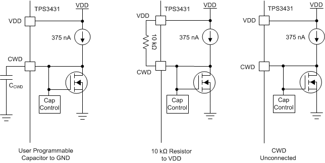
The TPS3431 features three options for setting the watchdog timeout: connecting a capacitor to the CWD pin, connecting a pull-up resistor to VDD, and leaving the CWD pin unconnected. Figure 8-1 shows a schematic drawing of all three options. If this pin is connected to VDD through a 10-kΩ pullup resistor or left unconnected (high impedance), then the factory-programmed watchdog timeouts are enabled; see the Section 8.1.1.1 section. Otherwise, the watchdog timeout can be adjusted by placing a capacitor from the CWD pin to ground.
GUID-DBA48489-470E-403A-9C9A-21D4F3D528B7-low.gifFigure 8-1 CWD Charging Circuit