SNVU695A June 2020 – January 2022 LP87702-Q1
3 Power Solution
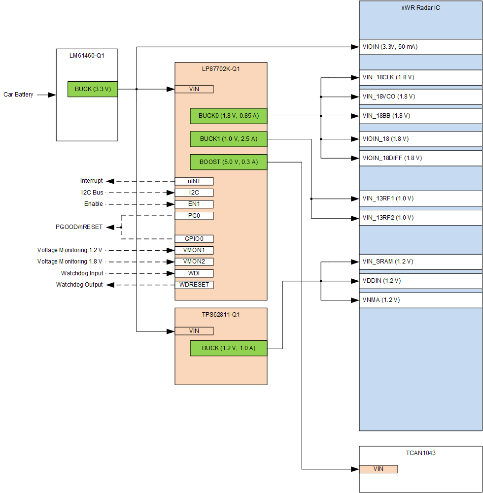
Figure 3-1 shows an example block diagram of LP87702K-Q1, wide VIN buck converter LM61460-Q1, TPS62811-Q1, and AWR or IWR radar IC device. The block diagram also includes a TCAN1043 CAN transceiver with CAN-FD.
 Figure 3-1 xWR Radar Input Power Tree Block Diagram
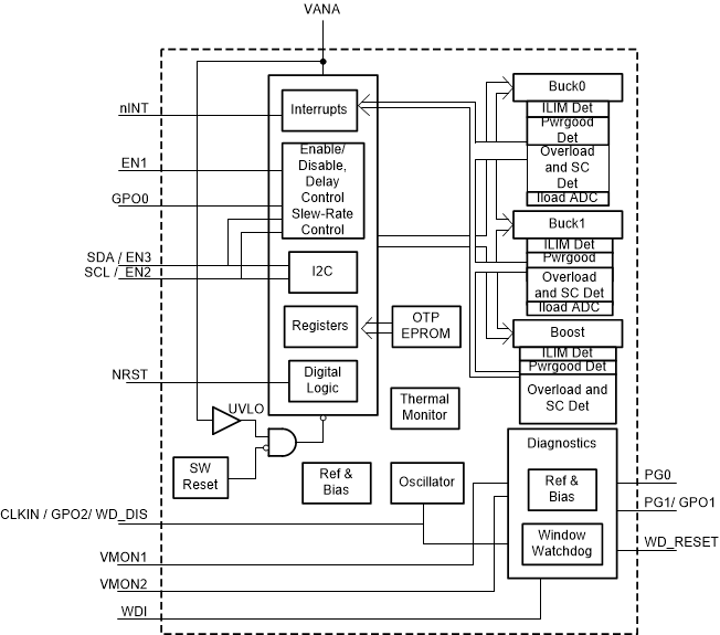
 Figure 3-2 LP87702x-Q1 Block Diagram
Figure 3-2 shows the functional block diagram of LP87702-Q1.
This radar sensor reference design is intended to connect directly to the vehicle battery and therefore the wide VIN controller is required. The following voltages required for the design are:
- 3.3 V for AWR1843 I/O—the LM61460-Q1 wide VIN buck converter covers a wide range of input voltages and can be used with a car battery (12 V typical) for example. LM61460-Q1 generates the 3.3 V rail and the device is also used as pre-regulator supply for other low voltage DC-DC converters. The preregulator switching frequency is set with an external resistor to be at 2.1 MHz. The 3.3 V output for radar is filtered with second LC filter even though the rail does not affect RF performance. However, there is a possibility of noise coupling at system level which could affect the RF performance and therefore a ferrite bead or a small inductor is used between the switching regulator output and radar supply rails.
- 1.2 V for AWR1843 digital and SRAM—the TPS62811-Q1 generates this supply from 3.3 V input. The switching frequency for TPS62811-Q1 is controlled with COMP/FSET pin and the switching frequency is set to 2.25 MHz. Similarly as with 3.3 V rail, 1.2 V rail does not have an immediate effect on RF performance but the noise coupling could affect performance. A second LC filter is used to improve this performance.
- 1.8 V for AWR1843 analog, RF, VCO, and CMOS—the LP87702K-Q1 BUCK0 generates this supply from 3.3 V input. The output is filtered with second LC filter stage.
- 1 V for AWR1843 analog and RF—the LP87702K-Q1 BUCK1 generates this supply from 3.3 V input.
- 5 V for CAN-FD PHY—the LP87702K-Q1 BOOST converter generates this supply from 3.3 V input.