SNVU699 October 2020
1.4 REF70EVM Board
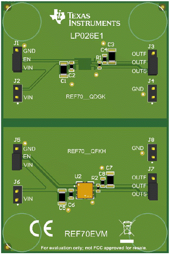
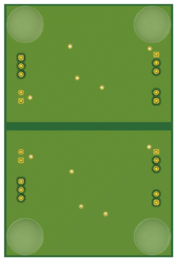
The PCB layout for the REF70EVM is illustrated in Figure 1-2 and Figure 1-3.
 Figure 1-2 REF70EVM Board Top
 Figure 1-3 REF70EVM Board Bottom
SNVU699 October 2020
The PCB layout for the REF70EVM is illustrated in Figure 1-2 and Figure 1-3.
 Figure 1-2 REF70EVM Board Top
 Figure 1-3 REF70EVM Board Bottom