SPRACN9E september 2022 – may 2023 AM67 , AM67A , AM68 , AM68A , AM69 , AM69A , DRA829J , DRA829J-Q1 , DRA829V , DRA829V-Q1 , TDA4AEN-Q1 , TDA4VEN-Q1 , TDA4VM , TDA4VM-Q1
- 1
- Jacinto 7 LPDDR4 Board Design and Layout Guidelines
- Trademarks
- 1Overview
-
2LPDDR4 Board Design and Layout Guidance
- 2.1 LPDDR4 Introduction
- 2.2 LPDDR4 Device Implementations Supported
- 2.3 LPDDR4 Interface Schematics
- 2.4 Compatible JEDEC LPDDR4 Devices
- 2.5 Placement
- 2.6 LPDDR4 Keepout Region
- 2.7 Net Classes
- 2.8 LPDDR4 Signal Termination
- 2.9 LPDDR4 VREF Routing
- 2.10 LPDDR4 VTT
- 2.11 CK and ADDR_CTRL Topologies
- 2.12 Data Group Topologies
- 2.13 CK and ADDR_CTRL Routing Specification
- 2.14 Data Group Routing Specification
- 2.15 Channel, Byte, and Bit Swapping
- 3LPDDR4 Board Design Simulations
- 4Revision History
3.6.2 Routing
The below examples show the LPDDR4 Clock and CA routing on an example 10 layer PCB design. The clock is routed differentially with target impedance of 70-ohms. For the T-branch to match the impedance of the trace, the impedance needs to be doubled. This can create challenges, as the higher impedances can be difficult to achieve in some PCB stackups. The CA signals are routed targeting 35-ohms, with the T-branch at two times the source impedance.
 Figure 3-8 Example LPDDR4 Clock and CA
Routing
Figure 3-8 Example LPDDR4 Clock and CA
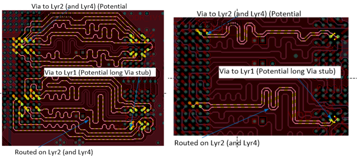
RoutingOn the same 10 layer reference design, the data groups are routed on layers 2 and 4. The upper layers are used due to the minimum via travel, which minimized the via inductance and via-to-via coupling. Because the data signals are point-to-point, T-branch routing is not required.
 Figure 3-9 Example LPDDR4 Data Byte(s)
and DQS(s) Routing
Figure 3-9 Example LPDDR4 Data Byte(s)
and DQS(s) Routing| Routing Layer | Via Type | Back Drilling | EW Margin (ps) | EH Margin (mV) |
|---|---|---|---|---|
| L1, L12 | PTH | No | -7.10 | 56.72 |
| L1, L12 | PTH | Yes | -4.86 | 55.71 |
| L1, L3 | PTH | No | 5.70 | 40.29 |
| L1, L3 | PTH | Yes | 8.37 | 34.54 |
| Routing Layer | Via Type | Back Drilling | EW Margin (ps) | EH Margin (mV) |
|---|---|---|---|---|
| L1, L12 | PTH | No | 17.42 | 39.22 |
| L1, L12 | PTH | Yes | 20.04 | 41.93 |
| L1, L3 | PTH | No | 27.66 | 41.37 |
| L1, L3 | PTH | Yes | 27.76 | 48.63 |