SPRACN9E september 2022 – may 2023 AM67 , AM67A , AM68 , AM68A , AM69 , AM69A , DRA829J , DRA829J-Q1 , DRA829V , DRA829V-Q1 , TDA4AEN-Q1 , TDA4VEN-Q1 , TDA4VM , TDA4VM-Q1
- 1
- Jacinto 7 LPDDR4 Board Design and Layout Guidelines
- Trademarks
- 1Overview
-
2LPDDR4 Board Design and Layout Guidance
- 2.1 LPDDR4 Introduction
- 2.2 LPDDR4 Device Implementations Supported
- 2.3 LPDDR4 Interface Schematics
- 2.4 Compatible JEDEC LPDDR4 Devices
- 2.5 Placement
- 2.6 LPDDR4 Keepout Region
- 2.7 Net Classes
- 2.8 LPDDR4 Signal Termination
- 2.9 LPDDR4 VREF Routing
- 2.10 LPDDR4 VTT
- 2.11 CK and ADDR_CTRL Topologies
- 2.12 Data Group Topologies
- 2.13 CK and ADDR_CTRL Routing Specification
- 2.14 Data Group Routing Specification
- 2.15 Channel, Byte, and Bit Swapping
- 3LPDDR4 Board Design Simulations
- 4Revision History
2.5 Placement
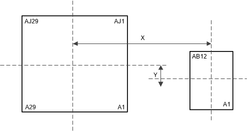
Figure 2-4 shows an example placement for the DRA829 processor and the LPDDR4 memory device. The recommended spacing parameters for all Jacinto7 devices and the LPDDR4 devices are defined in Table 2-3. The placement does not restrict the side of the PCB on which the devices are mounted. The ultimate purpose of the placement is to limit the maximum trace lengths and allow for proper routing space.
 Figure 2-4 DRA829 / LPDDR4 Example
Placement
Figure 2-4 DRA829 / LPDDR4 Example
PlacementTable 2-3 LPDDR4 Placement
Recommendations
| Number | Parameter | MIN | MAX | UNIT |
|---|---|---|---|---|
| 1 | X | 1200 | Mils | |
| 2 | Y | 250 | Mils |