SPRACV0A February 2021 – March 2023 F29H850TU , F29H850TU , F29H859TU-Q1 , F29H859TU-Q1 , TMS320F2800132 , TMS320F2800132 , TMS320F2800133 , TMS320F2800133 , TMS320F2800135 , TMS320F2800135 , TMS320F2800137 , TMS320F2800137 , TMS320F2800152-Q1 , TMS320F2800152-Q1 , TMS320F2800153-Q1 , TMS320F2800153-Q1 , TMS320F2800154-Q1 , TMS320F2800154-Q1 , TMS320F2800155 , TMS320F2800155 , TMS320F2800155-Q1 , TMS320F2800155-Q1 , TMS320F2800156-Q1 , TMS320F2800156-Q1 , TMS320F2800157 , TMS320F2800157 , TMS320F2800157-Q1 , TMS320F2800157-Q1 , TMS320F280021 , TMS320F280021 , TMS320F280021-Q1 , TMS320F280021-Q1 , TMS320F280023 , TMS320F280023 , TMS320F280023-Q1 , TMS320F280023-Q1 , TMS320F280023C , TMS320F280023C , TMS320F280025 , TMS320F280025 , TMS320F280025-Q1 , TMS320F280025-Q1 , TMS320F280025C , TMS320F280025C , TMS320F280025C-Q1 , TMS320F280025C-Q1 , TMS320F280033 , TMS320F280033 , TMS320F280034 , TMS320F280034 , TMS320F280034-Q1 , TMS320F280034-Q1 , TMS320F280036-Q1 , TMS320F280036-Q1 , TMS320F280036C-Q1 , TMS320F280036C-Q1 , TMS320F280037 , TMS320F280037 , TMS320F280037-Q1 , TMS320F280037-Q1 , TMS320F280037C , TMS320F280037C , TMS320F280037C-Q1 , TMS320F280037C-Q1 , TMS320F280038-Q1 , TMS320F280038-Q1 , TMS320F280038C-Q1 , TMS320F280038C-Q1 , TMS320F280039 , TMS320F280039 , TMS320F280039-Q1 , TMS320F280039-Q1 , TMS320F280039C , TMS320F280039C , TMS320F280039C-Q1 , TMS320F280039C-Q1 , TMS320F280040-Q1 , TMS320F280040-Q1 , TMS320F280040C-Q1 , TMS320F280040C-Q1 , TMS320F280041 , TMS320F280041 , TMS320F280041-Q1 , TMS320F280041-Q1 , TMS320F280041C , TMS320F280041C , TMS320F280041C-Q1 , TMS320F280041C-Q1 , TMS320F280045 , TMS320F280045 , TMS320F280048-Q1 , TMS320F280048-Q1 , TMS320F280048C-Q1 , TMS320F280048C-Q1 , TMS320F280049 , TMS320F280049 , TMS320F280049-Q1 , TMS320F280049-Q1 , TMS320F280049C , TMS320F280049C , TMS320F280049C-Q1 , TMS320F280049C-Q1 , TMS320F28075 , TMS320F28075 , TMS320F28075-Q1 , TMS320F28075-Q1 , TMS320F28076 , TMS320F28076 , TMS320F28374D , TMS320F28374D , TMS320F28374S , TMS320F28374S , TMS320F28375D , TMS320F28375D , TMS320F28375S , TMS320F28375S , TMS320F28375S-Q1 , TMS320F28375S-Q1 , TMS320F28376D , TMS320F28376D , TMS320F28376S , TMS320F28376S , TMS320F28377D , TMS320F28377D , TMS320F28377D-EP , TMS320F28377D-EP , TMS320F28377D-Q1 , TMS320F28377D-Q1 , TMS320F28377S , TMS320F28377S , TMS320F28377S-Q1 , TMS320F28377S-Q1 , TMS320F28378D , TMS320F28378D , TMS320F28378S , TMS320F28378S , TMS320F28379D , TMS320F28379D , TMS320F28379D-Q1 , TMS320F28379D-Q1 , TMS320F28379S , TMS320F28379S , TMS320F28384D , TMS320F28384D , TMS320F28384D-Q1 , TMS320F28384D-Q1 , TMS320F28384S , TMS320F28384S , TMS320F28384S-Q1 , TMS320F28384S-Q1 , TMS320F28386D , TMS320F28386D , TMS320F28386D-Q1 , TMS320F28386D-Q1 , TMS320F28386S , TMS320F28386S , TMS320F28386S-Q1 , TMS320F28386S-Q1 , TMS320F28388D , TMS320F28388D , TMS320F28388S , TMS320F28388S , TMS320F28P550SG , TMS320F28P550SG , TMS320F28P550SJ , TMS320F28P550SJ , TMS320F28P559SG-Q1 , TMS320F28P559SG-Q1 , TMS320F28P559SJ-Q1 , TMS320F28P559SJ-Q1 , TMS320F28P650DH , TMS320F28P650DH , TMS320F28P650DK , TMS320F28P650DK , TMS320F28P650SH , TMS320F28P650SH , TMS320F28P650SK , TMS320F28P650SK , TMS320F28P659DH-Q1 , TMS320F28P659DH-Q1 , TMS320F28P659DK-Q1 , TMS320F28P659DK-Q1 , TMS320F28P659SH-Q1 , TMS320F28P659SH-Q1
- Abstract
- Trademarks
-
1Introduction
- 1.1
Resources
- 1.1.1 TINA-TI SPICE-Based Analog Simulation Program
- 1.1.2 PSPICE for TI Design and Simulation Tool
- 1.1.3 Application Report: ADC Input Circuit Evaluation for C2000 MCUs
- 1.1.4 TI Precision Labs - SAR ADC Input Driver Design Series
- 1.1.5 Analog Engineer's Calculator
- 1.1.6 TI Precision Labs - Op Amps: Stability Series
- 1.1.7 TINA-TI ADC Input Models
- 1.1
Resources
-
2Charge-Sharing Concept
- 2.1 Traditional High-Speed ADC Driving Circuits
- 2.2 Increased Cs in High-Speed ADC Driving Circuits
- 2.3 Very Large Cs in ADC Driving Circuits
- 2.4 Charge-Sharing Operation
- 2.5 Sample Rate and Source Impedance vs. Tracking Error
- 2.6 Analytical Solution to Tracking Error
- 2.7 Charge-Sharing in Multiplexed ADCs
- 2.8 Charge-Sharing Circuit Advantages
- 2.9 Charge-Sharing Circuit Disadvantages
- 3Charge Sharing Design Flow
- 4Charge-Sharing Circuit Simulation Methods
- 5Example Circuit Designs
- 6Summary
- A Appendix: ADC Input Settling Motivation
- References
- Revision History
4.4 Measure the Settling Error
Once the circuit is built in TINA-TI, the steady-state voltage is measured (if applicable), and the sample rate is configured, measuring the settling error is relatively straightforward. This can be accomplished by running a transient analysis over enough periods to ensure that the system reaches steady state.
To run the transient analysis, use the TINA-TI commands "Analysis"→ "Transient..." then enter a simulation time period and select "OK". A good starting point is about 30 sampling periods.
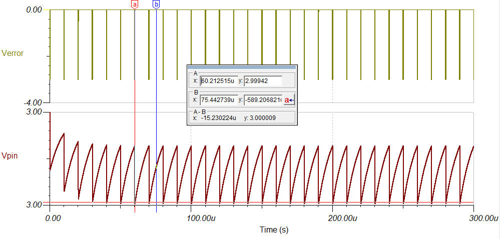
Figure 4-6 shows the results of this transient simulation applied to the example circuit in Figure 4-5 which has 100 nF Cs, 100Ω Rs , and a 100 kHz sampling rate. After simulation, signals were split into separate traces using the "View" → "Separate Curves" menu option. All traces other than Verror and Vpin were then deleted by selecting the curves and hitting the delete key.
To measure the total settling error, place a cursor at any point other than the S+H window on the Verror trace. This simulation shows about 589 µV of settling error from this method (cursor B). Alternately, the minimum value of Vpin can also be measured. This method shows approximately 3 V - 2.99942 V = 580 µV of settling error (cursor A).
 Figure 4-6 Settling Error
Measurement
Figure 4-6 Settling Error
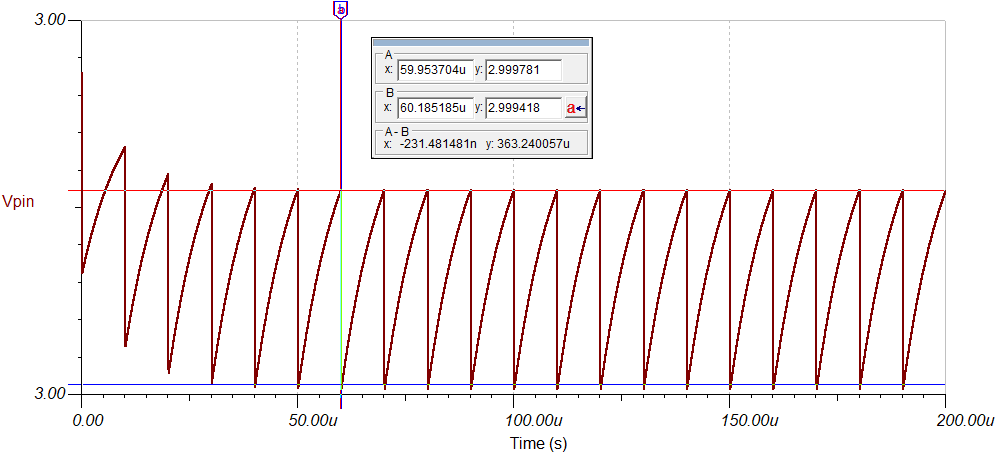
MeasurementIn addition, it is possible to separately measure the charge-share and tracking errors. Figure 4-7 shows the results of narrowing the simulation to 20 periods and also deleting the Verror trace. The distance from 3 V to max value of Vpin in steady state is the approximate tracking error. In this case, the tracking error is 3 V - 2.999781 V = 219 µV (cursor A). Similarly, the charge-share error is the difference between the tracking error point and the minimum pin voltage in the steady state. In this case, the charge-share error is 2.99781 V - 2.999418 V = 363 µV (cursor A minus cursor A).
 Figure 4-7 Settling Error Component
Measurement