SPRACW9A June 2021 – March 2023 F29H850TU , F29H850TU , F29H859TU-Q1 , F29H859TU-Q1 , TMS320F2800132 , TMS320F2800132 , TMS320F2800133 , TMS320F2800133 , TMS320F2800135 , TMS320F2800135 , TMS320F2800137 , TMS320F2800137 , TMS320F2800152-Q1 , TMS320F2800152-Q1 , TMS320F2800153-Q1 , TMS320F2800153-Q1 , TMS320F2800154-Q1 , TMS320F2800154-Q1 , TMS320F2800155 , TMS320F2800155 , TMS320F2800155-Q1 , TMS320F2800155-Q1 , TMS320F2800156-Q1 , TMS320F2800156-Q1 , TMS320F2800157 , TMS320F2800157 , TMS320F2800157-Q1 , TMS320F2800157-Q1 , TMS320F280021 , TMS320F280021 , TMS320F280021-Q1 , TMS320F280021-Q1 , TMS320F280023 , TMS320F280023 , TMS320F280023-Q1 , TMS320F280023-Q1 , TMS320F280023C , TMS320F280023C , TMS320F280025 , TMS320F280025 , TMS320F280025-Q1 , TMS320F280025-Q1 , TMS320F280025C , TMS320F280025C , TMS320F280025C-Q1 , TMS320F280025C-Q1 , TMS320F280033 , TMS320F280033 , TMS320F280034 , TMS320F280034 , TMS320F280034-Q1 , TMS320F280034-Q1 , TMS320F280036-Q1 , TMS320F280036-Q1 , TMS320F280036C-Q1 , TMS320F280036C-Q1 , TMS320F280037 , TMS320F280037 , TMS320F280037-Q1 , TMS320F280037-Q1 , TMS320F280037C , TMS320F280037C , TMS320F280037C-Q1 , TMS320F280037C-Q1 , TMS320F280038-Q1 , TMS320F280038-Q1 , TMS320F280038C-Q1 , TMS320F280038C-Q1 , TMS320F280039 , TMS320F280039 , TMS320F280039-Q1 , TMS320F280039-Q1 , TMS320F280039C , TMS320F280039C , TMS320F280039C-Q1 , TMS320F280039C-Q1 , TMS320F280040-Q1 , TMS320F280040-Q1 , TMS320F280040C-Q1 , TMS320F280040C-Q1 , TMS320F280041 , TMS320F280041 , TMS320F280041-Q1 , TMS320F280041-Q1 , TMS320F280041C , TMS320F280041C , TMS320F280041C-Q1 , TMS320F280041C-Q1 , TMS320F280045 , TMS320F280045 , TMS320F280048-Q1 , TMS320F280048-Q1 , TMS320F280048C-Q1 , TMS320F280048C-Q1 , TMS320F280049 , TMS320F280049 , TMS320F280049-Q1 , TMS320F280049-Q1 , TMS320F280049C , TMS320F280049C , TMS320F280049C-Q1 , TMS320F280049C-Q1 , TMS320F28075 , TMS320F28075 , TMS320F28075-Q1 , TMS320F28075-Q1 , TMS320F28076 , TMS320F28076 , TMS320F28374D , TMS320F28374D , TMS320F28374S , TMS320F28374S , TMS320F28375D , TMS320F28375D , TMS320F28375S , TMS320F28375S , TMS320F28375S-Q1 , TMS320F28375S-Q1 , TMS320F28376D , TMS320F28376D , TMS320F28376S , TMS320F28376S , TMS320F28377D , TMS320F28377D , TMS320F28377D-EP , TMS320F28377D-EP , TMS320F28377D-Q1 , TMS320F28377D-Q1 , TMS320F28377S , TMS320F28377S , TMS320F28377S-Q1 , TMS320F28377S-Q1 , TMS320F28378D , TMS320F28378D , TMS320F28378S , TMS320F28378S , TMS320F28379D , TMS320F28379D , TMS320F28379D-Q1 , TMS320F28379D-Q1 , TMS320F28379S , TMS320F28379S , TMS320F28384D , TMS320F28384D , TMS320F28384D-Q1 , TMS320F28384D-Q1 , TMS320F28384S , TMS320F28384S , TMS320F28384S-Q1 , TMS320F28384S-Q1 , TMS320F28386D , TMS320F28386D , TMS320F28386D-Q1 , TMS320F28386D-Q1 , TMS320F28386S , TMS320F28386S , TMS320F28386S-Q1 , TMS320F28386S-Q1 , TMS320F28388D , TMS320F28388D , TMS320F28388S , TMS320F28388S , TMS320F28P650DH , TMS320F28P650DH , TMS320F28P650DK , TMS320F28P650DK , TMS320F28P650SH , TMS320F28P650SH , TMS320F28P650SK , TMS320F28P650SK , TMS320F28P659DH-Q1 , TMS320F28P659DH-Q1 , TMS320F28P659DK-Q1 , TMS320F28P659DK-Q1 , TMS320F28P659SH-Q1 , TMS320F28P659SH-Q1
- Abstract
- Trademarks
-
1Introduction
- 1.1 Memory Cross-Talk Challenges
- 1.2
Resources for Signal Conditioning Circuit
Design
- 1.2.1 TI Precision Labs - SAR ADC Input Driver Design Series
- 1.2.2 Analog Engineer's Calculator
- 1.2.3 Related Application Reports
- 1.2.4 TINA-TI SPICE-Based Analog Simulation Program
- 1.2.5 PSPICE for TI
- 1.2.6 ADC Input Circuit Evaluation for C2000 MCUs
- 1.2.7 Charge-Sharing Driving Circuits for C2000 ADCs
- 2Review of ADC Input Settling
- 3Problem Statement
- 4Dedicated ADC Sampling
- 5Pre-Sampling VREFLO
- 6Summary
- 7References
- 8Revision History
4.2 Settling Mechanism for Dedicated ADC
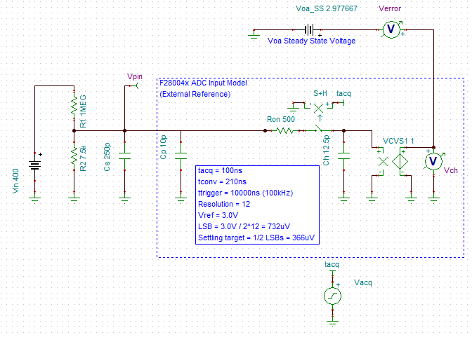
Figure 4-2 shows the setup for a simulation of the first few periods of settling for the example system rearranged as described in Dedicated ADC Concept. A 100ns S+H window will be used, which is much shorter than the time previously determined to be necessary for good settling under normal conditions (11.8 µs). Note that the portion of the input model which discharges the S+H capacitor between samples has been removed, so CH will retain its charge between samples. Finally, note that the simulation is configured such that the initial voltage condition on CH is 0 V while the voltage divider output is a voltage near full-scale (3.0 V). This will result in a simulation equivalent to a full-scale input setup.
 Figure 4-2 Simulation Schematic for V2 on
Dedicated ADC
Figure 4-2 Simulation Schematic for V2 on
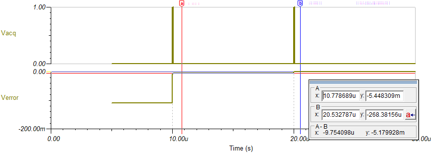
Dedicated ADCRunning a transient simulation for 30µs gives the results as shown in figure Figure 4-3. The settling error after the first sample is about 100 mV, which is then reduced to 5.4 mV and then 0.27 mV after the second and third samples, respectively. Since 1/2 LSB settling with a 3.0 V ADC range is about 0.37 mV, the system did eventually achieve good settling in response to a full-scale step response! However, this took three sample periods (30 µs) and assumed that the signal remained stationary after the step response.
 Figure 4-3 Settling Simulation for V2 Circuit on
Dedicated ADC
Figure 4-3 Settling Simulation for V2 Circuit on
Dedicated ADCWhat is quite interesting about these results is that 11.8 µs of settling time was predicted as necessary for this circuit topology, but the ADC only had the S+H window open for three bursts of 100 ns, resulting in 300 ns of total sampling time. How then did the circuit achieve good settling?
For each sample, note that the error scales down by roughly a factor of 20. This corresponds to the ratio of the external ADC input capacitor, CS (250 pF in this case), to the internal ADC S+H capacitor, CH (12.5 pF in this case). When the S+H first opens, these two capacitors quickly equalize, charging CH 95% of the way towards the input voltage present on CS.