SPRACZ0A August 2021 – March 2023 F29H850TU , F29H850TU , F29H859TU-Q1 , F29H859TU-Q1 , TMS320F2800132 , TMS320F2800132 , TMS320F2800133 , TMS320F2800133 , TMS320F2800135 , TMS320F2800135 , TMS320F2800137 , TMS320F2800137 , TMS320F2800152-Q1 , TMS320F2800152-Q1 , TMS320F2800153-Q1 , TMS320F2800153-Q1 , TMS320F2800154-Q1 , TMS320F2800154-Q1 , TMS320F2800155 , TMS320F2800155 , TMS320F2800155-Q1 , TMS320F2800155-Q1 , TMS320F2800156-Q1 , TMS320F2800156-Q1 , TMS320F2800157 , TMS320F2800157 , TMS320F2800157-Q1 , TMS320F2800157-Q1 , TMS320F280021 , TMS320F280021 , TMS320F280021-Q1 , TMS320F280021-Q1 , TMS320F280023 , TMS320F280023 , TMS320F280023-Q1 , TMS320F280023-Q1 , TMS320F280023C , TMS320F280023C , TMS320F280025 , TMS320F280025 , TMS320F280025-Q1 , TMS320F280025-Q1 , TMS320F280025C , TMS320F280025C , TMS320F280025C-Q1 , TMS320F280025C-Q1 , TMS320F280033 , TMS320F280033 , TMS320F280034 , TMS320F280034 , TMS320F280034-Q1 , TMS320F280034-Q1 , TMS320F280036-Q1 , TMS320F280036-Q1 , TMS320F280036C-Q1 , TMS320F280036C-Q1 , TMS320F280037 , TMS320F280037 , TMS320F280037-Q1 , TMS320F280037-Q1 , TMS320F280037C , TMS320F280037C , TMS320F280037C-Q1 , TMS320F280037C-Q1 , TMS320F280038-Q1 , TMS320F280038-Q1 , TMS320F280038C-Q1 , TMS320F280038C-Q1 , TMS320F280039 , TMS320F280039 , TMS320F280039-Q1 , TMS320F280039-Q1 , TMS320F280039C , TMS320F280039C , TMS320F280039C-Q1 , TMS320F280039C-Q1 , TMS320F280040-Q1 , TMS320F280040-Q1 , TMS320F280040C-Q1 , TMS320F280040C-Q1 , TMS320F280041 , TMS320F280041 , TMS320F280041-Q1 , TMS320F280041-Q1 , TMS320F280041C , TMS320F280041C , TMS320F280041C-Q1 , TMS320F280041C-Q1 , TMS320F280045 , TMS320F280045 , TMS320F280048-Q1 , TMS320F280048-Q1 , TMS320F280048C-Q1 , TMS320F280048C-Q1 , TMS320F280049 , TMS320F280049 , TMS320F280049-Q1 , TMS320F280049-Q1 , TMS320F280049C , TMS320F280049C , TMS320F280049C-Q1 , TMS320F280049C-Q1 , TMS320F28075 , TMS320F28075 , TMS320F28075-Q1 , TMS320F28075-Q1 , TMS320F28076 , TMS320F28076 , TMS320F28374D , TMS320F28374D , TMS320F28374S , TMS320F28374S , TMS320F28375D , TMS320F28375D , TMS320F28375S , TMS320F28375S , TMS320F28375S-Q1 , TMS320F28375S-Q1 , TMS320F28376D , TMS320F28376D , TMS320F28376S , TMS320F28376S , TMS320F28377D , TMS320F28377D , TMS320F28377D-EP , TMS320F28377D-EP , TMS320F28377D-Q1 , TMS320F28377D-Q1 , TMS320F28377S , TMS320F28377S , TMS320F28377S-Q1 , TMS320F28377S-Q1 , TMS320F28378D , TMS320F28378D , TMS320F28378S , TMS320F28378S , TMS320F28379D , TMS320F28379D , TMS320F28379D-Q1 , TMS320F28379D-Q1 , TMS320F28379S , TMS320F28379S , TMS320F28384D , TMS320F28384D , TMS320F28384D-Q1 , TMS320F28384D-Q1 , TMS320F28384S , TMS320F28384S , TMS320F28384S-Q1 , TMS320F28384S-Q1 , TMS320F28386D , TMS320F28386D , TMS320F28386D-Q1 , TMS320F28386D-Q1 , TMS320F28386S , TMS320F28386S , TMS320F28386S-Q1 , TMS320F28386S-Q1 , TMS320F28388D , TMS320F28388D , TMS320F28388S , TMS320F28388S , TMS320F28P550SG , TMS320F28P550SG , TMS320F28P550SJ , TMS320F28P550SJ , TMS320F28P559SG-Q1 , TMS320F28P559SG-Q1 , TMS320F28P559SJ-Q1 , TMS320F28P559SJ-Q1 , TMS320F28P650DH , TMS320F28P650DH , TMS320F28P650DK , TMS320F28P650DK , TMS320F28P650SH , TMS320F28P650SH , TMS320F28P650SK , TMS320F28P650SK , TMS320F28P659DH-Q1 , TMS320F28P659DH-Q1 , TMS320F28P659DK-Q1 , TMS320F28P659DK-Q1 , TMS320F28P659SH-Q1 , TMS320F28P659SH-Q1
- Abstract
- Trademarks
-
1Introduction
- 1.1
Resources
- 1.1.1 TINA-TI SPICE-Based Analog Simulation Program
- 1.1.2 PSPICE for TI Design and Simulation Tool
- 1.1.3 Application Report: ADC Input Circuit Evaluation for C2000 MCUs
- 1.1.4 TI Precision Labs - SAR ADC Input Driver Design Series
- 1.1.5 Analog Engineer's Calculator
- 1.1.6 TI Precision Labs - Op Amps: Stability Series
- 1.1.7 Related Application Reports
- 1.1.8 Comparison of Schematic Capture and Simulation Tools
- 1.1.9 PSpice for TI ADC Input Models
- 1.1
Resources
-
2Charge-Sharing Concept
- 2.1 Traditional High-Speed ADC Driving Circuits
- 2.2 Increased Cs in High-Speed ADC Driving Circuits
- 2.3 Very Large Cs in ADC Driving Circuits
- 2.4 Charge-Sharing Operation
- 2.5 Sample Rate and Source Impedance vs. Tracking Error
- 2.6 Analytical Solution to Tracking Error
- 2.7 Charge-Sharing in Multiplexed ADCs
- 2.8 Charge-Sharing Circuit Advantages
- 2.9 Charge-Sharing Circuit Disadvantages
- 3Charge Sharing Design Flow
- 4Charge-Sharing Circuit Simulation Methods
- 5Example Circuit Designs
- 6Summary
- A Appendix: ADC Input Settling Motivation
- References
- Revision History
2.6 Analytical Solution to Tracking Error
In a charge-sharing design, the total settling error is made up of two error components: the charge-sharing error and the tracking error. The charge-sharing error is determined by the relative sizes of the source capacitance, Cs, and the ADC's internal S+H capacitance, CH. The tracking error is determined by the ability of the source to recharge Cs through the external source resistance, Rs, in the time between samples. Since the recharge primarily occurs while the ADC sampling switch is open, a first-order exponential RC settling model is appropriate where the RC time constant, τ, is determined by Rs and Cs.
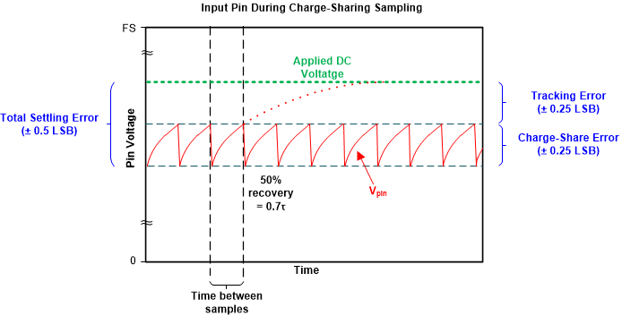
To simplify analysis, it is assumed that the total settling error budget is equally divided between charge-sharing error and tracking error. In the case of a total settling error budget of 0.5 LSBs, the target for each of the sub-components would be 0.25 LSBs. Regardless of the absolute magnitude of the error components, allowing 50% recovery in the time between samples results in equal error component magnitudes (equivalent to approximately 0.7 RC time constants). The equal error magnitudes in equilibrium are illustrated in Figure 2-7. At the beginning of each sample, charge equalizes between Cs and CH, resulting in a 0.25 LSBs drop in voltage. Then, in the time until the next conversion, the pin voltage charges exponentially back towards the applied DC voltage. Recovering from 0.5 LSBs to 0.25 LSBs requires 50% settling.
 Figure 2-7 Charge Sharing Steady State With
DC Input
Figure 2-7 Charge Sharing Steady State With
DC InputSince the criteria for equal error components requires 0.7 time constants, the following equation determines the approximate maximum sample rate given a fixed source impedance:
Alternately, if a specific sample rate is required, the above equation can be rearranged to give the maximum source impedance for a known sample rate:
For example, consider a circuit with 12.5 pF CH, target sample rate of 10 ksps, and settling error target of 0.5 LSBs at 12-bit resolution. To get charge sharing error of 0.25 LSBs, Cs will be set to approximately 12.5 pF⋅(4096/0.25) = 204.8 nF. This will then yield a maximum source impedance of: