SWRA465A August 2014 – July 2015 CC2530 , CC2530 , CC2530-RF4CE , CC2530-RF4CE , CC2592 , CC2592
- Using CC2592 Front End With CC2530
- A Marker - Delta Method
- Revision History
7.1 Compliance of FCC Part 15.247 When Using the CC2530 With the CC2592
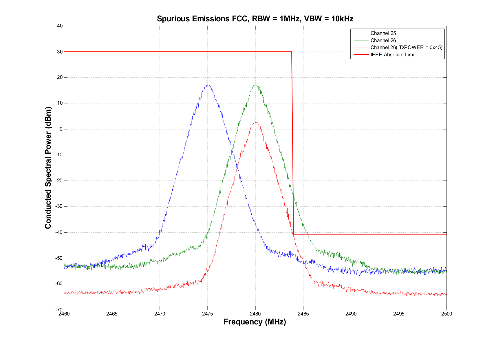
When using CC2592 with the CC2530 a back-off is required for the highest IEEE 802.15.4 channel (channel 26) to comply with FCC. Table 9 shows the back-off needed to comply with the FCC Part 15.247 limits at typical conditions. Note that the numbers in Table 9 are based on conducted emission measurements from the CC2530 - CC2592EM reference design. The real required back-off may be different for applications with different antennas, plastic covers, or other factors that amplify or attenuate the radiated power.
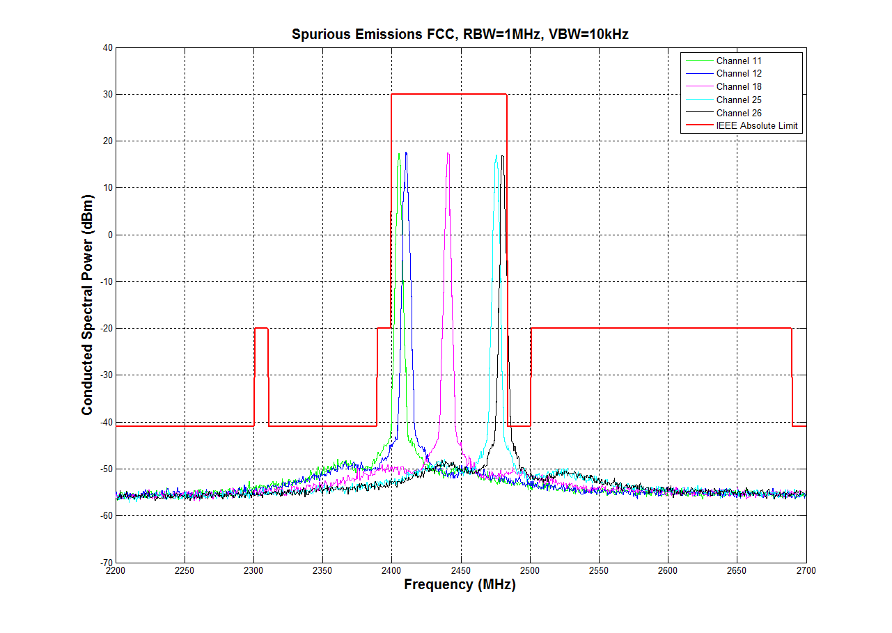
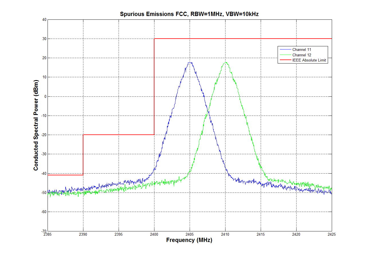
Figure 9 depicts the level of the conducted spurious emission and margins to the FCC Part 15.247 limits for the IEEE 802.15.4 channels under typical conditions (TC = 25°C, VDD = 3.0 V) when transmitting at maximum recommended power (TXPOWER = 0xE5) using the CC2530 - CC2592EM. Figure 10 and Figure 11 show the margins versus the FCC 15.247 for the lowest frequency channels at the lower band edge and for the upper frequency channels at the upper band edge respectively. At the band edge the FCC allows for a Marker-delta method of measurement to determine the amount of back off or duty cycle required to comply with the FCC Part 15.247. This is necessary because when making radiated band-edge measurements, there can be an issue obtaining meaningful data since a measurement instrument that is tuned to a band-edge frequency may also capture some of the in-band signal when using the resolution bandwidth (RBW) required by measurement procedure ANSI C63.4-1992. Section A provides a step-by-step example of using the marker-delta method to calculate the required back off required.
Table 9. Back-Off Requirement for FCC Part 15.247 Compliance Under Typical Conditions
| Frequency [MHz] | Back-Off [dB] |
|---|---|
| 2405 | 0 |
| 2410 | 0 |
| 2415 | 0 |
| 2420 | 0 |
| 2425 | 0 |
| 2430 | 0 |
| 2435 | 0 |
| 2440 | 0 |
| 2445 | 0 |
| 2450 | 0 |
| 2455 | 0 |
| 2460 | 0 |
| 2465 | 0 |
| 2470 | 0 |
| 2475 | 0 |
| 2480 | 12 |
 Figure 9. Conducted Spurious Emission vs. FCC Part 15.247 Limit (TXPOWER = 0xE5, RBW = 1 MHz, VBW = 10 kHz)
  Figure 10. Conducted Spurious Emission, Lower Band Edge (TXPOWER = 0xE5, RBW = 1 MHz,
VBW = 10 KHz)
 Figure 11. Conducted Spurious Emission, Upper Band Edge (TXPOWER = 0xE5, RBW = 1 MHz,
VBW = 10 KHz)