SWRA636C November 2019 – December 2020 CC1352P , CC2652P
A.1 Schematic
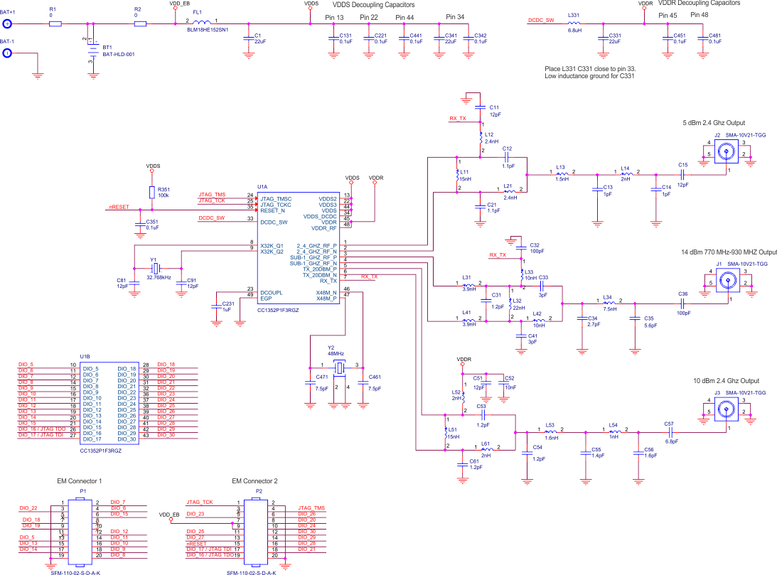
Figure 6-1 shows the schematic for the board used for testing. Only the 10 dBm 2.4 Ghz path has been tested on this specific board.
 Figure 6-1 CC1352PEM-XD7793-XD24-PA24_10dBm Schematic