SWRS262B February   2021  – September 2022 CC2652RSIP

PRODUCTION DATA  

  1. Features
  2. Applications
  3. Description
  4. Functional Block Diagram
  5. Revision History
  6. Device Comparison
  7. Terminal Configuration and Functions
    1. 7.1 Pin Diagram
    2. 7.2 Signal Descriptions – SIP Package
    3. 7.3 Connections for Unused Pins and Modules
  8. Specifications
    1. 8.1  Absolute Maximum Ratings
    2. 8.2  ESD Ratings
    3. 8.3  Recommended Operating Conditions
    4. 8.4  Power Supply and Modules
    5. 8.5  Power Consumption - Power Modes
    6. 8.6  Power Consumption - Radio Modes
    7. 8.7  Nonvolatile (Flash) Memory Characteristics
    8. 8.8  Thermal Resistance Characteristics
    9. 8.9  RF Frequency Bands
    10. 8.10 Bluetooth Low Energy - Receive (RX)
    11. 8.11 Bluetooth Low Energy - Transmit (TX)
    12. 8.12 Zigbee and Thread - IEEE 802.15.4-2006 2.4 GHz (OQPSK DSSS1:8, 250 kbps) - RX
    13. 8.13 Zigbee and Thread - IEEE 802.15.4-2006 2.4 GHz (OQPSK DSSS1:8, 250 kbps) - TX
    14. 8.14 Timing and Switching Characteristics
      1. 8.14.1 Reset Timing
      2. 8.14.2 Wakeup Timing
      3. 8.14.3 Clock Specifications
        1. 8.14.3.1 48 MHz Crystal Oscillator (XOSC_HF)
        2. 8.14.3.2 48 MHz RC Oscillator (RCOSC_HF)
        3. 8.14.3.3 2 MHz RC Oscillator (RCOSC_MF)
        4. 8.14.3.4 32.768 kHz Crystal Oscillator (XOSC_LF)
        5. 8.14.3.5 32 kHz RC Oscillator (RCOSC_LF)
      4. 8.14.4 Synchronous Serial Interface (SSI) Characteristics
        1. 8.14.4.1 Synchronous Serial Interface (SSI) Characteristics
        2.       36
      5. 8.14.5 UART
        1.       38
    15. 8.15 Peripheral Characteristics
      1. 8.15.1 ADC
        1.       Analog-to-Digital Converter (ADC) Characteristics
      2. 8.15.2 DAC
        1. 8.15.2.1 Digital-to-Analog Converter (DAC) Characteristics
      3. 8.15.3 Temperature and Battery Monitor
        1. 8.15.3.1 Temperature Sensor
        2. 8.15.3.2 Battery Monitor
      4. 8.15.4 Comparators
        1. 8.15.4.1 Low-Power Clocked Comparator
        2. 8.15.4.2 Continuous Time Comparator
      5. 8.15.5 Current Source
        1. 8.15.5.1 Programmable Current Source
      6. 8.15.6 GPIO
        1. 8.15.6.1 GPIO DC Characteristics
    16. 8.16 Typical Characteristics
      1. 8.16.1 MCU Current
      2. 8.16.2 RX Current
      3. 8.16.3 TX Current
      4. 8.16.4 RX Performance
      5. 8.16.5 TX Performance
      6. 8.16.6 ADC Performance
  9. Detailed Description
    1. 9.1  Overview
    2. 9.2  System CPU
    3. 9.3  Radio (RF Core)
      1. 9.3.1 Bluetooth 5.2 Low Energy
      2. 9.3.2 802.15.4 (Thread, Zigbee, 6LoWPAN)
    4. 9.4  Memory
    5. 9.5  Sensor Controller
    6. 9.6  Cryptography
    7. 9.7  Timers
    8. 9.8  Serial Peripherals and I/O
    9. 9.9  Battery and Temperature Monitor
    10. 9.10 µDMA
    11. 9.11 Debug
    12. 9.12 Power Management
    13. 9.13 Clock Systems
    14. 9.14 Network Processor
    15. 9.15 Device Certification and Qualification
      1. 9.15.1 FCC Certification and Statement
      2. 9.15.2 IC/ISED Certification and Statement
      3. 9.15.3 ETSI/CE Certification
      4. 9.15.4 UK Certification
    16. 9.16 Module Markings
    17. 9.17 End Product Labeling
    18. 9.18 Manual Information to the End User
  10. 10Application, Implementation, and Layout
    1. 10.1 Application Information
      1. 10.1.1 Typical Application Circuit
    2. 10.2 Device Connection and Layout Fundamentals
      1. 10.2.1 Reset
      2. 10.2.2 Unused Pins
    3. 10.3 PCB Layout Guidelines
      1. 10.3.1 General Layout Recommendations
      2. 10.3.2 RF Layout Recommendations
        1. 10.3.2.1 Antenna Placement and Routing
        2. 10.3.2.2 Transmission Line Considerations
    4. 10.4 Reference Designs
    5. 10.5 Junction Temperature Calculation
  11. 11Environmental Requirements and SMT Specifications
    1. 11.1 PCB Bending
    2. 11.2 Handling Environment
      1. 11.2.1 Terminals
      2. 11.2.2 Falling
    3. 11.3 Storage Condition
      1. 11.3.1 Moisture Barrier Bag Before Opened
      2. 11.3.2 Moisture Barrier Bag Open
    4. 11.4 PCB Assembly Guide
      1. 11.4.1 PCB Land Pattern & Thermal Vias
      2. 11.4.2 SMT Assembly Recommendations
      3. 11.4.3 PCB Surface Finish Requirements
      4. 11.4.4 Solder Stencil
      5. 11.4.5 Package Placement
      6. 11.4.6 Solder Joint Inspection
      7. 11.4.7 Rework and Replacement
      8. 11.4.8 Solder Joint Voiding
    5. 11.5 Baking Conditions
    6. 11.6 Soldering and Reflow Condition
  12. 12Device and Documentation Support
    1. 12.1 Device Nomenclature
    2. 12.2 Tools and Software
      1. 12.2.1 SimpleLink™ Microcontroller Platform
    3. 12.3 Documentation Support
    4. 12.4 Support Resources
    5. 12.5 Trademarks
    6. 12.6 Electrostatic Discharge Caution
    7. 12.7 Glossary
  13. 13Mechanical, Packaging, and Orderable Information
    1. 13.1 Packaging Information

Transmission Line Considerations

The RF signal from the module is routed to the antenna using a Coplanar Waveguide with ground (CPW-G) structure. CPW-G structure offers the maximum amount of isolation and the best possible shielding to the RF lines. In addition to the ground on the L1 layer, placing GND vias along the line also provides additional shielding.

Figure 10-3 shows a cross section of the coplanar waveguide with the critical dimensions.

Figure 10-4 shows the top view of the coplanar waveguide with GND and via stitching.
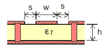
GUID-D026ACAE-C872-4BF7-BC8C-2CC223D4F5DF-low.gif Figure 10-3 Coplanar Waveguide (Cross Section)
GUID-6F9EEE09-9A88-40C7-B0AF-D735652AEF5B-low.gif Figure 10-4 CPW With GND and Via Stitching (Top View)

The recommended values for a 4-layer PCB board is provided in Table 10-4.

Table 10-4 Recommended PCB Values for 4-Layer Board (L1 to L2 = 0.175 mm)
PARAMETER VALUE UNITS
W 0.300 mm
S 0.500 mm
H 0.175 mm
Er (FR-4 substrate) 4.0 F/m