TIDUAY6E November 2015 – March 2020
4.1.1.1 Base Board Settings
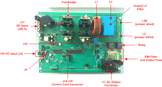
This reference design follows an HSEC control card concept, and any device for which the HSEC control card is available from the C2000 MCU product family can be potentially used on the design. The key resources used for controlling the power stage on the MCU are listed in Table 3. Figure 15 shows the key power stage and connectors on the reference design, and Table 4 lists the key connectors and their functions. To get started:
- Confirm that no power source is connected to the design.
- Confirm that the output filter is correct for the mode that the device will run in. For example, voltage source inverter uses an LC filter. The L2 and L2N slot must be jumper wired as shown in Figure 11.
- Ensure that the capacitor is 20 µF by checking the marking on the capacitor.
- Insert the control card in the J15-J16 slot.
- Insert a jumper at J10 if not already populated.
- Connect a 15-V DC, 1-A power supply at J2.
- Insert a jumper at J4 if not already populated. The LED lights on the base board and control card will light up to indicate that the device is powered up.
- To connect JTAG, use a USB cable from the control card and connect it to a host computer.
- A DC source can also be connected to the J17, but do not apply power at this point.
- Connect a resistive load of approximately 100 Ω to the output from J1.
NOTE
The bias for the MCU is separated from the power stage, enabling safe bring up of the system.
 Figure 15. Board Overview
 Table 3. Key Controller Peripherals Used for Control on the Full Bridge on the Board
| SIGNAL NAME | HSEC PIN NUMBER | FUNCTION |
|---|---|---|
| PWM-1A | 49 | PWM: Inverter drive |
| PWM-1B | 51 | PWM: Inverter drive |
| PWM-2A | 53 | PWM: Inverter drive |
| PWM-2B | 55 | PWM: Inverter drive |
| I.inv | 15 | ADC: Inductor current measurement |
| 1.65V | 17 | ADC: Reference voltage generated on the board |
| Bus.V | 21 | ADC: DC bus sensed on the board |
| Line.V | 25 | ADC: AC voltage sensing |
| PLC_RX | 27, 12 | ADC: PLC ADC pin |
| SD_Data_CapI | 99 | SDFM: Data from the SDFM modulator for the capacitor current feedback |
| SD_Data_GridI | 103 | SDFM: Data from the SDFM modulator for output current |
| SD_Data_Vbus | 100 | SDFM: Data from the SDFM modulator for the DC bus voltage |
| SD_Data_GridV | 107 | SDFM: Data from the SDFM modulator for the grid voltage |
| SD_CLK_GridV /
SD_CLK_GridI / SD_CLK_CapI |
50, 101, 105, 109 | SDFM: Data from the SDFM modulator for the grid voltage |
| SD_CLK_Vbus | 102, 54 | SDFM: Clock from the SDFM modulator used for Vbus measurement. The clock is generated from ECAP1 module which is brought out using the output xBar |
| OPRLY | 52 | GPIO: relay gpio output |
| SW-ON | 56 | GPIO: switch gpio input |
Table 4. Key Connectors and Their Function
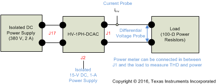
Figure 16 shows a block diagram of a typical setup of this reference design under test.
 Figure 16. Hardware Setup to Run Software