TIDUAY6E November 2015 – March 2020
4.1.2.3.3 Running the Code
- Run the project by clicking the
 button.
 - Clear the inverter trip by setting the clearlnvTrip variable to 1.
- Set the rlyConnect variable to 1 to connect the relay.
- Set a small current command of 0.02 for invliRef.
- Slowly raise the DC bus.
- Observe the invIiInst rises slowly, and then regulates at the value set by invliRef.
- For the 100-Ω output load, the inverter will begin regulating the current once the DC bus is raised about 50 V. Increasing the DC Bus further will not result in increase in the invIiInst, which verifies closed loop operation.
- Once the closed loop operation is verified, for example, invlireflnst closely matches invliRef, the DC bus must be raised to the operating voltage, such as 380 V.
- After raising the DC bus to 380 V, the invliRef must be increased in steps of 0.02 pu to 0.08 pu, while continually monitoring closed loop operation (that is, with invIiInst matched invIiRef at every step change, one can monitor these on the oscilloscope as well to verify settling time, overshoot, and so on).
- This design at 380-V DC input with 0.08-pu current invIiRef set will correspond to approximately 1.3 Amps of current in case of SDFM monitored using a guiIi variable, which with a 100-Ω load, will equal 170 W of power.
- To run the SFRA, keep the project running and from the CFG page, click on the SFRA icon.
- SFRA GUI will appear.
- Select the options for the device on the GUI; for example, for TMS320F28377D, select floating point.
- Click on setup connection.
- On the pop-up window, uncheck the boot on connect option.
- Select an appropriate COM port, and click OK.
- Return to the SFRA GUI.
- Click connect.
- The SFRA GUI will connect to the device.
- A SFRA sweep can now be started by clicking on Start Sweep.
- The complete SFRA sweep will take a few minutes to complete.
- Activity may be monitored by viewing the progress bar on the SFRA GUI, and also by checking the flashing of the blue LED light on the back of the control card that indicates UART activity.
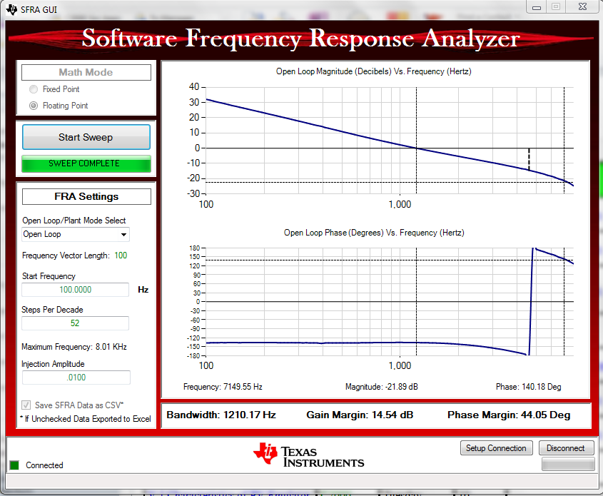
- Once complete, a graph will open a loop plot, as shown in Figure 29. This verifies that the designed compensator is stable.
- Click on the Compensation Designer from the SYSCFG page.
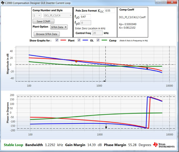
- Choose SFRA Data for the plant option on the GUI. This will use the measured plant information to design the compensator. This option must be used to fine tune the compensation.
- If a previous SFRA run plant information needs to be used, the user must select the SFRAData.csv file by browsing to it.
- Click on Browse SFRA Data.
- Close Compensation Designer to return to the syscfg page.
- The current compensator design has been verified.
- Set the invliRef to zero.
- Reduce the DC bus to zero.
- Disconnect the relay by setting rlyConnect to zero.
- Fully halting the MCU when in real-time mode is a two step process.
- First, halt the processor by clicking
 on the toolbar, or by using Target→Halt.
 - Take the MCU out of real-time mode by clicking on
 .
. - Finally, reset the MCU by clicking on
 .
. - Close the CCS debug session by clicking on Terminate Debug Session
 , or by using Target → Terminate all.
NOTE
If the closed loop operation is not verified, the user must reduce the DC bus immediately, and verify Build 1 to see if all the voltage and current sensing parameters are correct. The user must also visit the compensation designer again to verify that the system has enough gain at DC.
NOTE
SFRA is integrated in the software of this build to verify the designed compensator provides enough gain and phase margin by measuring on hardware.
If these blue LEDs stop blinking, it indicates a loss of communication. Under this situation, close SFRA GUI, and restart the connection process. If the situation persists, bring the system to a safe stop by setting the invIiRef to 0 and bringing the DC bus voltage down to 0. Terminate the debug session, followed by connecting and reconnecting the JTAG USB cable to reset the JTAG circuit and relaunch a debug session by following the steps outlined previously to rerun the SFRA.
 Figure 29. SFRA Run on Closed Current Loop
 The frequency response data is also saved in the project folder under an SFRA Data Folder, and is time stamped with the time of the SFRA run.
The measured gain and phase margin are better than the modeled values, indicating slight differences in modeled and measured response. In this case, the difference is of gain reduction which decreases the bandwidth, but improves the margins. However, depending on the estimate of the parameters of the power stage, the margins may shift either way and it is essential to measure the response to ensure robust operation.
For the voltage source inverter, TI recommends to keep the crossover of the inner current loop at greater than ten times the AC frequency, which is met by this compensator, and no changes are needed in the design. If an adapted solution is not met, the compensator must be changed to ensure the crossover of the current loop meets this requirement.
NOTE
By default, the compensation designer will point to the latest SFRA run.
Figure 30 shows the compensation designer with measured plant frequency response data.
