TIDUCJ0G November 2016 – April 2020
5.1 Base Board Settings
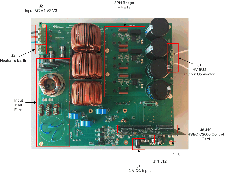
The design follows a HSEC control card concept. Any device for which a HSEC control card is available from the C2000 MCU product family can be potentially used on this design. The key resources used for controlling the power stage on the MCU are listed in Table 2. Figure 15 shows the key power stage and connectors on the design guide, and Table 3 lists the key connectors and their functions. To get started:
- Make sure no power source is connected to the design.
- Insert the control card in the J8-J10 slot.
- Insert a jumper at J11 and J12 to connect the bias supply for 5 V and 3.3 V .
- Connect a 12-V DC, 1-Amps power supply at J4. A few LEDs on the base board will light up indicating power. The LED on the control card will also light up. This light indicates the device is powered up as well.
- To connect JTAG, use a USB cable from the control card and connect it into a host computer.
- A three-phase power supply is connected to the input J2. The board works as a three-wire system, therefore, the connection of the neutral is not required. A virtual neutral is generated on the board for sensing purpose of VL-N voltages.
- A resistive load of approximately 500Ω should also be connected to the output at J1. The load is connected across the positive and negative terminal (Vbus). The midpoint (M) is not connected to the load.
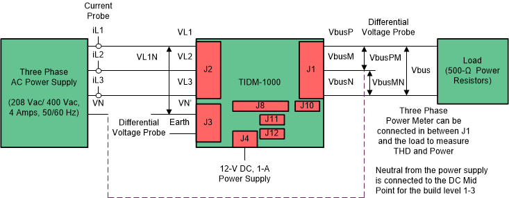
- Current and voltage probes can be connected to observe the input current, input voltage, and output voltages, as shown in Figure 16.
NOTE
The bias for the MCU is separated from the power stage, which enables safe bring up of the system.
Figure 15. Board Overview

Table 2. Key Controller Peripherals Used for Control of Power Stage on Board
| SIGNAL NAME | HSEC PIN NUMBER | FUNCTION |
|---|---|---|
| PWM-1A | 49 | PWM: Vienna rectifier PWM Ph1A |
| PWM-1B | 51 | PWM: Vienna rectifier PWM Ph1B |
| PWM-2A | 53 | PWM: Vienna rectifier PWM Ph2A |
| PWM-2B | 55 | PWM: Vienna rectifier PWM Ph2B |
| PWM-3A | 50 | PWM: Vienna rectifier PWM Ph3A |
| PWM-3B | 52 | PWM: Vienna rectifier PWM Ph3B |
| IL1 | 15, 20 | ADC with CMPSS: Inductor current measurement Ph1 |
| IL2 | 21.27 | ADC with CMPSS: Inductor current measurement Ph2 |
| IL3 | 25 | ADC with CMPSS: Inductor current measurement Ph3 |
| V1 | 18 | ADC: AC voltage sensing Ph1 |
| V2 | 28 | ADC: AC voltage sensing Ph2 |
| V3 | 34 | ADC: AC voltage sensing Ph3 |
| Vbus_PM | 31, 24 | ADC: Bus voltage positive terminal to midpoint |
| Vbus_MN | 37, 26 | ADC: Bus voltage midpoint to negative terminal |
| Profiling GPIO1 | 58 | GPIO: Used to profile code (optional) |
| Profiling GPIO2 | 60 | GPIO: Used to profile code (optional) |
Table 3. Key Connectors and Function
Figure 16. Hardware Setup to Run Software
