TIDUCU8A september 2022 – may 2023
3.3.2 Interface Wake-Up Voltages (TCM_PHYL_INTF_IQWUH and TCM_PHYL_INTF_IQWUHL)
The next tests verify the behavior of the IO-Link CQ lines driver stage during the generation of a wake-up pulse. The CQ output is loaded with a resistive load resulting in a 500-mA current and the voltage level is observed. The first two tests verify the high-side driver.
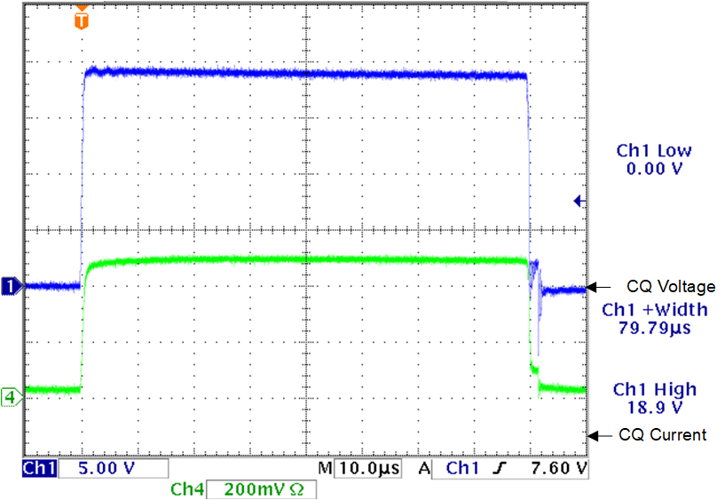
 Figure 3-3 TCM_PHYL_INTF_IQWUH With 20
V
Figure 3-3 TCM_PHYL_INTF_IQWUH With 20
VThe first test is shown in Figure 3-3. Here, the supply voltage is set to 20 V and the line is loaded with 40 Ω, resulting in 500 mA of current. It is observed if the voltage level exceeds VTHHmax which is 13 V. The scope plot shows a measurement of 18.9 V, so this test is passed.
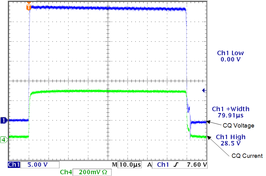
 Figure 3-4 TCM_PHYL_INTF_IQWUH With 30
V
Figure 3-4 TCM_PHYL_INTF_IQWUH With 30
VSimilar measurement has to be done with a supply voltage of 30 V, the scope plot in Figure 3-4 shows this. Here the resistive load has to be changed to 60 Ω, so the resulting current is still 500 mA. A voltage of 28.5 V is measured, so this test is also passed.
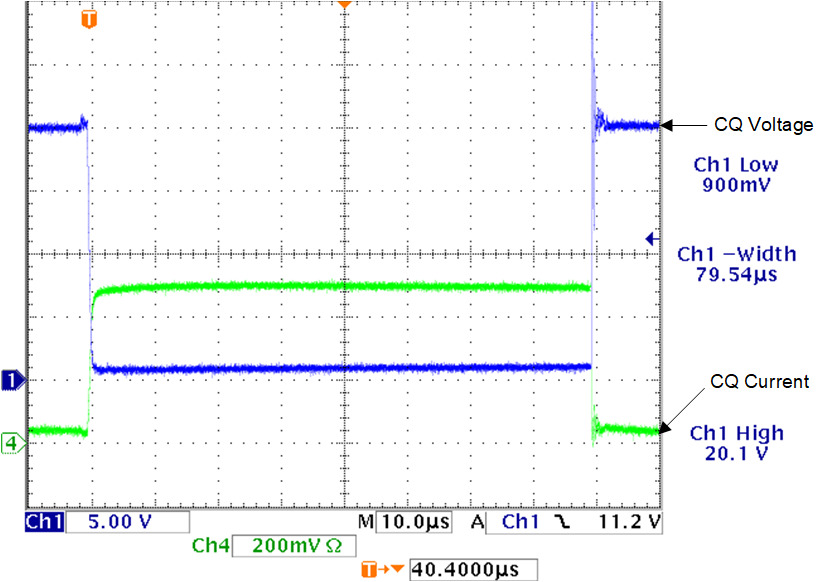
 Figure 3-5 TCM_PHYL_INTF_IQWUL With 20
V
Figure 3-5 TCM_PHYL_INTF_IQWUL With 20
VThe same test is to be done for the low side driver. Figure 3-5 shows the first test with a supply voltage of 20 V. Again the line has to be loaded with a resistive load resulting in 500 mA. In this case, the load is connected to L+. As illustrated, a voltage of 0.9 V is measured, which is a pass for this test.
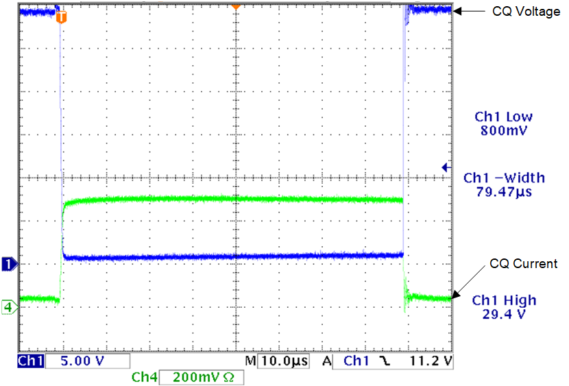
 Figure 3-6 TCM_PHYL_INTF_IQWUL With 30
V
Figure 3-6 TCM_PHYL_INTF_IQWUL With 30
VThe last physical layer test is similar but with 30 V and an equally higher load resistor. The results in Figure 3-6 show again a voltage of 0.9 V. Which is again a pass.
Table 3-1 lists all physical layer tests in summary and the results.
| ID | Name | Configuration | Specification (Clause) | Comment | Result |
|---|---|---|---|---|---|
| SDCI_TC_0001 | TCM_PHYL_INTF_ISM | The supply current at the Master port is monitored. | See Section 5.3.2.3, Table 6 in IO-Link Interface and System Specification Version 1.1.34 | Test with 500 mA | 20 V: Pass 30 V: Pass |
| SDCI_TC_0002 | TCM_PHYL_INTF_ISIRM | The supply current at the Master port is monitored. | Test with 500 mA | 20 V: Pass 30 V: Pass |
|
| SDCI_TC_0003 | TCM_PHYL_INTF_ILLM | The input current at C/Q at the Master port is monitored. | ILLM (VIM = 5 V, VSM = 20 V):
8.56mA Pass ILLM (VIM = 5,1 V, VSM = 20 V): 8.56 mA Pass ILLM (VIM = 15 V, VSM = 20 V): 8.57 mA Pass ILLM (VIM = VSM = 20 V): 8.57 mA Pass ILLM (VIM = 5 V, VSM = 30 V): 8.57 mA Pass ILLM (VIM = 5,1 V, VSM = 30 V): 8.57 mA Pass ILLM (VIM = 15 V, VSM = 30 V): 8.58 mA Pass ILLM (VIM = VSM = 30 V): 8.59 mA Pass |
||
| SDCI_TC_0004 | TCM_PHYL_INTF_VREShigh | The output level at the Master C/Q output is measured. | VRQHM (VSM = 20 V): 0.23 V VRQHM (VSM = 30 V): 0.228 V Pass |
||
| SDCI_TC_0005 | TCM_PHYL_INTF_VRESLOW | The output level at the Master C/Q output is measured. | VRQLM (VSM = 20 V): 0.225 V VRQLM (VSM = 30 V): 0.225 V Pass |
||
| SDCI_TC_0006 | TCM_PHYL_INTF_VTHHM | The digital input signal for C/Q input is monitored | See Section 5.3.2.2, Table 5 in IO-Link Interface and System Specification Version 1.1.34 | VIM@VTHHM (VSM = 20 V): 11.1 V
VIM@VTHHM (VSM = 30 V): 11.1 V Pass |
|
| SDCI_TC_0007 | TCM_PHYL_INTF_VTHLM | The digital input signal for C/Q input is monitored | VIM@VTHLM (VSM = 20 V): 10.35 V
VIM@VTHLM (VSM = 30 V): 10.35 V Pass |
||
| SDCI_TC_0008 | TCM_PHYL_INTF_VHYSM | Comparison of values from SDCI_TC_0006 and SDCI_TC_0007 | VHYSM (VSM = 20 V): 0.75 V VHYSM (VSM = 30 V): 0.75 V Pass |
||
| SDCI_TC_0299 | TCM_PHYL_INTF_VOLTRANGECQ | Test if working after connecting CQ to 0 V and 30 V via 1 Ω | See Section 5.3.2.2, Table 5 - VIL and VIH, in IO-Link Interface and System Specification Version 1.1.34 | Pass | |
| SDCI_TC_0021 | TCM_PHYL_INTF_IQWUH | See Section 5.3.3.3, Table 9 in IO-Link Interface and System Specification Version 1.1.34 | Wake-up pulse from function generator | VIM@WURQ (VSM = 20 V): 18.9 V
VIM@WURQ (VSM = 30 V): 28.5 V Pass |
|
| SDCI_TC_0022 | TCM_PHYL_INTF_TWUH | Wake-up pulse from function generator | TWUH@WURQ (VSM = 20 V): 80 µs
TWUH@WURQ (VSM = 30 V): 80 µs Pass |
||
| SDCI_TC_0023 | TCM_PHYL_INTF_IQWUL | Wake-up pulse from function generator | VIM@WURQ (VSM = 20 V): 0.9 V
VIM@WURQ (VSM = 30 V): 0.9 V Pass |
||
| SDCI_TC_0024 | TCM_PHYL_INTF_TWUL | Wake-up pulse from function generator | TWUL@WURQ (VSM = 20 V): 80 µs
TWUL@WURQ (VSM = 30 V): 80 µs Pass |