TIDUDI9A January 2018 – May 2025 ISOM8610
- 1
- Description
- Resources
- Features
- Applications
- 6
- 1System Description
- 2System Overview
- 3Hardware, Software, Testing Requirements, and Test Results
- 4Design Files
- 5Software Files
- 6Related Documentation
- 7About the Author
- 8Revision History
2.3.2.2 Case 2: Wire Intact and Input State '0'
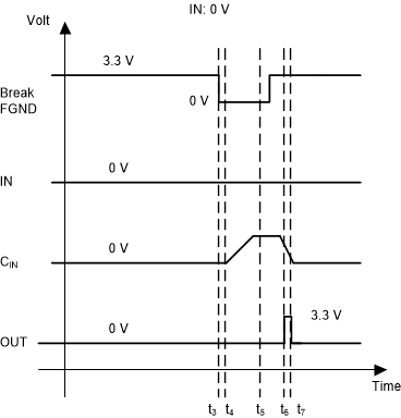
In case the wire in intact and IN is '0', OUT is '0' as long as Break FNGD is '1'. As soon as Break FNGD is '0' (t3), the field ground of the ISO121x is disconnected. Now, CIN is charged to the supply voltage of the field device. This result is because the field device has a pullup resistor to its supply and it is still connected to CIN (t4). Again, consider the delay of the optical switch.
Because the ISO121x has no ground connection, there is no voltage drop across the device. This result means that the voltage at CIN is also present at the floating FGND pin of the ISO121x. Hence, the voltage drop across the optical switch (equal pin FGND and field ground) is also equal to the supply voltage of the field device.
Break FGND can switch to '1' again when CIN is charged to the supply voltage of the field device (t5). As soon as the ISO121x is connected to the field ground again, the device starts operating. The ISO121x is now supplied by the energy stored in CIN. As soon as the current through the sense resistor RSENSE is high enough (IMIN = 2.2 mA, taken from the ISO121x data sheet) and the voltage at the SENSE pin is above the voltage level threshold, OUT switches to '1' (t6). As soon as the voltage level at CIN drops below the voltage level threshold for a high state, OUT drops back to '0' (t7).
The curves of IN and CIN would be identical because they are connected to each other. However, to indicate that the digital output state of the field device is '0' continuously, IN is '0' in the diagram continuously as well.
 Figure 2-9 Broken Wire Detection With
Intact Wire and IN = 0 V