TIDUDO6B May 2019 – October 2020
- Description
- Resources
- Features
- Applications
- 5
- 1System Description
-
2System Overview
- 2.1 Block Diagram
- 2.2 Highlighted Products
- 2.3
System Design Theory and Design Considerations
- 2.3.1 AFE4900 and Power Supply
- 2.3.2 CC2640R2F Microcontroller
- 2.3.3 PPG Measurement
- 2.3.4 ECG Measurement
- 2.3.5 Selecting TX Supply (TX_SUP) Value for Driving LEDs
- 2.3.6 Generating TX Supply for Driving LEDs
- 2.3.7 Generating RX Supply for AFE4900
- 2.3.8 Generating I/O Supply
- 2.3.9 Battery Input and Reservoir Capacitors
- 2.3.10 Battery Life Calculations
- 2.3.11 External Memory
- 2.3.12 LED Indications
- 2.3.13 Connections Between Sensor Board and ECG Board
-
3Hardware, Software, Testing Requirements, and Test Results
- 3.1 Required Hardware and Software
- 3.2 Testing and Results
-
4Design Files
- 4.1 Schematics
- 4.2 Bill of Materials
- 4.3
PCB Layout Recommendations
- 4.3.1 Layout for Main Board
- 4.3.2 Connection From PDs to AFE
- 4.3.3 Connections From LEDs to AFE
- 4.3.4 Connections From ECG PADs to AFE
- 4.3.5 Connections Between BT and AFE
- 4.3.6 Connections Between BT Antenna and Chip
- 4.3.7 Boost Converter
- 4.3.8 Buck-Boost Converter
- 4.3.9 Layouts for PPG Sensor Boards
- 4.3.10 Layout for ECG Sensor Board
- 4.3.11 Layout Prints
- 4.4 Altium Project
- 4.5 Gerber Files
- 4.6 Assembly Drawings
- 5Software Files
- 6Related Documentation
- 7About the Authors
- Revision History
2.3.1 AFE4900 and Power Supply
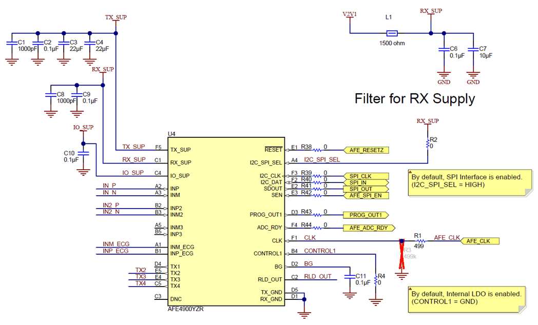
Figure 2-2 shows different connections for the AFE4900 device.
The AFE4900 device needs three power supplies: TX_SUP, RX_SUP, and IO_SUP. TX_SUP (4.2 V) is generated using the TPS61099 device. RX_SUP (2.1 V) is generated using the TPS63036 device. IO_SUP is the same as RX_SUP.
For PPG measurement, the LEDs are driven using the TX2, TX3, and TX4 pins (TX1 is not connected in the design). The reflected signals are detected using PDs connected to the INP-INM and INP2-INM2 pins (INP3-INM3 pins are not connected in the design).
For ECG measurement, the signals coming from electrodes are connected to the INP_ECG and INM_ECG pins. The right-leg drive signal is available on RLD_OUT pin.
The BG pin is connected to the internal bandgap voltage. The BG pin is decoupled using a 0.1-µF capacitor (C11) on the board.
 Figure 2-2 AFE4900 Connections Schematic
For the AFE4900 device, RX_SUP is filtered using an LC filter consisting of the ferrite bead L1 and capacitors C6 and C7.
Table 2-1 lists the connections between the AFE4900 and CC2640R2F devices.
| AFE4900 PIN NUMBER | FUNCTION | CC2640R2F PIN NUMBER | FUNCTION | COMMENTS |
|---|---|---|---|---|
| E1 | /RESET | 6 | DIO_1 | Reset for the AFE |
| A4 | I2C_SPI_SEL | N/A | N/A | Selection between SPI and I2C. For this design, SPI is selected, so this pin is connected to RX_SUP through a 0-Ω resistor (R2). |
| F3 | I2C_CLK | 16 | DIO_10 | SPI_CLK |
| F2 | I2C_DAT | 14 | DIO_8 | SPI_IN |
| E2 | SDOUT | 15 | DIO_9 | SPI_OUT |
| E3 | SEN | 5 | DIO_0 | AFE_SPI_EN |
| D3 | PROG_OUT1 | 21 | DIO_15 | |
| F4 | ADC_RDY | 28 | DIO_18 | ADC ready signal |
| F1 | CLK | 29 | DIO_19 | AFE clock |
| B4 | CONTROL1 | N/A | N/A | Enables or disables the internal LDO. For this design, the internal LDO is enabled, so this pin is connected to GND through a 0-Ω resistor (R4). |