TIDUDS9B December 2017 – November 2022
- Description
- Resources
- Features
- Applications
- 5
- 1System Description
-
2System Overview
- 2.1 Block Diagram
- 2.2
Design Considerations
- 2.2.1 Conditions of Use: Assumption
- 2.2.2
Diagnostics Coverage
- 2.2.2.1 Dual-Channel Monitoring
- 2.2.2.2 Checking ISO1211 Functionality With MCU (SIL1)
- 2.2.2.3 Checking TPS22919 Functionality With MCU (SIL1)
- 2.2.2.4 Checking TPS27S100 Functionality With MCU (SIL1)
- 2.2.2.5 Optional Monitoring Using RDY Pin of ISO5452, ISO5852S or UCC21750 Integrated Analog-to-PWM Isolated Sensor
- 2.2.3 Drive State
- 2.3 Highlighted Products
- 2.4 System Design Theory
-
3Hardware, Software, Testing Requirements, and Test Results
- 3.1 Getting Started Hardware
- 3.2 Testing and Results
- 4Design Files
- 5Related Documentation
- 6About the Author
- 7Recognition
- 8Revision History
3.2.3.4 Inrush Current Measurement
Set the current limit with the TPS27S00 device. As mentioned in Section 2.4.3, the current limit is set to 1 A. The current during the peak is limited to 1 A, as calculated in Equation 8.
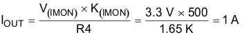
Calculate the current in the switch during the ON state using Equation 9.
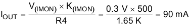
This calculated value for IOUT matches well with the value measured by the multimeter (see Figure 3-15 and Figure 3-16).
 Figure 3-15 Inrush Current Measurement From
TPS27S100
Figure 3-15 Inrush Current Measurement From
TPS27S100 Figure 3-16 Zoomed-In Shot of Inrush Current Measurement
From TPS27S100
Figure 3-16 Zoomed-In Shot of Inrush Current Measurement
From TPS27S100The two peaks that Figure 3-15 and Figure 3-16 show during the transition state corresponds to the current limit due to the input and output capacitance of the TIDA-00199 board. Path 1 and path 2 in Figure 3-17 show the two capacitances charging on the TIDA-00199 board.