TIDUDS9B December 2017 – November 2022
- Description
- Resources
- Features
- Applications
- 5
- 1System Description
-
2System Overview
- 2.1 Block Diagram
- 2.2
Design Considerations
- 2.2.1 Conditions of Use: Assumption
- 2.2.2
Diagnostics Coverage
- 2.2.2.1 Dual-Channel Monitoring
- 2.2.2.2 Checking ISO1211 Functionality With MCU (SIL1)
- 2.2.2.3 Checking TPS22919 Functionality With MCU (SIL1)
- 2.2.2.4 Checking TPS27S100 Functionality With MCU (SIL1)
- 2.2.2.5 Optional Monitoring Using RDY Pin of ISO5452, ISO5852S or UCC21750 Integrated Analog-to-PWM Isolated Sensor
- 2.2.3 Drive State
- 2.3 Highlighted Products
- 2.4 System Design Theory
-
3Hardware, Software, Testing Requirements, and Test Results
- 3.1 Getting Started Hardware
- 3.2 Testing and Results
- 4Design Files
- 5Related Documentation
- 6About the Author
- 7Recognition
- 8Revision History
2.4.2 STO_1 Signal Flow Path for Controlling VCC1
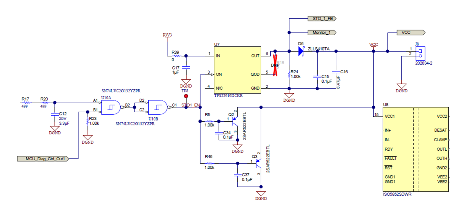
The TPS22919 is a small, ultra-low leakage current, single-channel load switch. Figure 2-11 shows the schematic design of the TPS22860.
 Figure 2-11 TPS22919 Schematic
The device power supply is 3.3 V which is assumed to be protected against fault and remains within ±20% tolerance. To limit the voltage drop on the input supply, which is caused by transient inrush currents when the switch turns on into a discharged load capacitor, a ceramic capacitor of 1 µF is placed between the VIN and GND pins.
The ON pin which is compatible with standard GPIO logic threshold controls the state of the switch by signal STO1_EN. The QOD pin is left open, the output will be floating when ON pin is logic low.
Use Equation 5 to calculate the inrush current during turn on for a given capacitance and slew rate:

The output of the switch is connected to the primary 3.3-V supply (VCC) of the gate driver. Dual redundant PNP bipolar junction transistors Q2 and Q3, actively clamp the logic side gate drive supply VCC to GND when STO_1 is activated. This prevents reverse bias of the VCC supply through the CMOS input gate driver ISO5852S (or ISO5452) in case the PWM signals are still active high (3V3).