TIDUDS9B December 2017 – November 2022
- Description
- Resources
- Features
- Applications
- 5
- 1System Description
-
2System Overview
- 2.1 Block Diagram
- 2.2
Design Considerations
- 2.2.1 Conditions of Use: Assumption
- 2.2.2
Diagnostics Coverage
- 2.2.2.1 Dual-Channel Monitoring
- 2.2.2.2 Checking ISO1211 Functionality With MCU (SIL1)
- 2.2.2.3 Checking TPS22919 Functionality With MCU (SIL1)
- 2.2.2.4 Checking TPS27S100 Functionality With MCU (SIL1)
- 2.2.2.5 Optional Monitoring Using RDY Pin of ISO5452, ISO5852S or UCC21750 Integrated Analog-to-PWM Isolated Sensor
- 2.2.3 Drive State
- 2.3 Highlighted Products
- 2.4 System Design Theory
-
3Hardware, Software, Testing Requirements, and Test Results
- 3.1 Getting Started Hardware
- 3.2 Testing and Results
- 4Design Files
- 5Related Documentation
- 6About the Author
- 7Recognition
- 8Revision History
3.1.1 PCB Overview
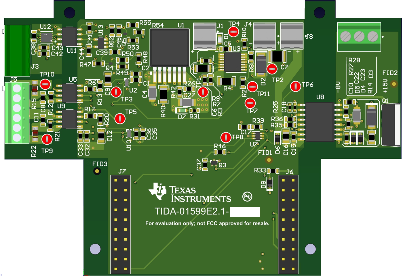
Figure 3-1 shows a top view of the printed-circuit board (PCB) with RevE2.1
 Figure 3-1 TIDA-01599 PCB - Top
View
Figure 3-1 TIDA-01599 PCB - Top
ViewJ5 is a six-pin connector, which provides an input to the two 24-V STO signals. J3 is a five-pin connector, which provides the 24-V power supply from safe PLC and also feedback the STO_FB signal to safe PLC. J1 is a 24-V connector, which powers up the high-side load switch. The 3.3-V rail is generated on the board, which supplies power to the digital isolator, AND Gate, low-side switch, and MCU. J4 and J8 are the connectors which supply 24 V and 3.3 V, respectively, from the output of the two switches.
J6 and J7 are female connectors, which have been set 52-mm apart for interfacing to the C2000™ MCU LaunchPad™ Development Kit.
Table 3-1 through Table 3-4 list the pin assignments, pin description and levels of all the connectors used in TIDA-01599 reference design.
| PIN | SIGNAL | SPECIFICATION | COMMENT |
|---|---|---|---|
J5-1 |
STO_2 |
24-V for STO_2 input |
|
J5-2 |
GND2 |
24-V input GND2 |
|
J5-3 |
GND1 |
24-V input GND1 | |
J5-4 |
STO_1 |
24-V for STO_1 input | |
J5-5 |
NC |
||
J5-6 |
NC |
| PIN | SIGNAL | SPECIFICATION | COMMENT |
|---|---|---|---|
J3-1 |
Safe PLC 24V |
24-V power supply from safe PLC |
|
J3-2 |
NC |
||
J3-3 |
STO_FB |
STO feedback signal with logic high 24-V and logic low 0-V |
|
J3-4 |
NC |
||
J3-5 |
COM |
Reference GND of safe PLC 24-V |
| PIN | SIGNAL | SPECIFICATION | COMMENT |
|---|---|---|---|
J1-1 |
DGND |
24-V input DGND |
|
J1-2 |
24VIN |
24-V input |
|
J4-1 |
P24V |
24-V output |
STO_2 output |
J4-2 |
DGND |
24-V output DGND |
|
J8-1 |
VCC |
3.3-V output |
STO_1 output |
| J8-2 | DGND | 3.3-V output DGND |
| PIN | SIGNAL | SPECIFICATION | COMMENT |
|---|---|---|---|
J6-1 |
P3V3 |
3.3-V output |
|
J6-2 |
NC | ||
J6-3 |
NC | ||
J6-4 |
DGND |
DGND for 3.3-V amd I/Os |
|
J6-5 |
MCU_STO2_In | 3.3-V output from ISO1211 for STO_2 channel | For ISO1211 diagnostic |
J6-6 |
Monitor_1 | 3.3-V output from TPS22919 for STO_1 channel | For TPS22919 diagnostic |
J6-7 |
MCU_Diag_Ctrl_Out1 | 3.3-V logic high pulse from SIL 1 MCU | Diagnostic pulse to turn off the safety switch 1 |
J6-8 |
Monitor_2 | 2.8-V output from TPS27S100 for STO_2 channel | For TPS27S100 diagnostic |
J6-9 |
MCU_Diag_Ctrl_Out2 | 3.3-V logic high pulse from SIL 1 MCU | Diagnostic pulse to turn off the safety switch 2 |
J6-10 |
NC | ||
J6-11 |
NC | ||
J6-12 |
NC | ||
J6-13 |
RDY |
Power-good output of gate driver, connect to 3.3-V with pull up resistor | Active high when both supplies are good |
J6-14 |
NC |
||
J6-15 |
FLT |
Fault output of gate driver, connect to 3.3-V with pull up resistor | Active-low during DESAT condition |
J6-16 |
NC |
||
J6-17 |
RST |
Reset input of gate driver (Logic high 3.3-V) | Apply a low pulse to reset fault latch |
J6-18 |
NC |
||
J6-19 |
CS |
Current-monitor output of TPS27S100, connect to MCU ADC input with voltage range 0-V to 3.3-V | |
J6-20 |
NC |
||
J7-1 |
PWW_In |
PWM Pulse from MCU (Logic low 0-V, Logic high 3.3-V) | |
J7-2 |
DGND |
DGND for I/Os |
|
J7-3 |
NC | ||
J7-4 |
NC | ||
J7-5 |
NC | ||
J7-6 |
NC | ||
J7-7 |
NC | ||
J7-8 |
NC | ||
J7-9 |
NC | ||
J7-10 |
NC | ||
J7-11 |
NC | ||
J7-12 |
NC | ||
J7-13 |
MCU_STO1_In |
3.3-V output from ISO1211 for STO_1 channel | For ISO1211 diagnostic |
J7-14 |
NC | ||
J7-15 |
DIAG_EN | Enable and disable pin of TPS27S100 for diagnostic functions | The enable pin is permanently connected to 3.3-V to enable continuous diagnostic monitoring and also send back to the diagnostic MCU (SIL 1) |
J7-16 |
NC |
||
J7-17 |
NC | ||
J7-18 |
NC | ||
J7-19 |
NC | ||
J7-20 |
NC |