TIDUE82A November 2021 – April 2024
2.4.1 Inverting Power Supply Design Using TPS62933
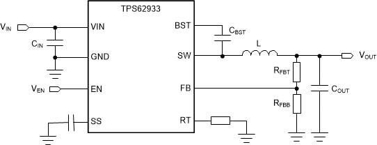
The inverting buck-boost topology is similar to the buck topology. In the buck configuration, shown in Figure 2-2, the positive connection (VOUT) is connected to the inductor, and the return connection is connected to the integrated circuit (IC) ground (GND). However, in Figure 2-1 illustrating the inverting buck-boost configuration, the IC GND is used as the negative output voltage pin. What was the positive output in the buck configuration is used as the GND. This inverting topology allows the output voltage to be inverted and always lower than the GND.
 Figure 2-2 Buck Converter
Application
Figure 2-2 Buck Converter
ApplicationThe circuit operation in the inverting buck-boost topology is different from the buck topology. During the on time of the control MOSFET, the inductor is charged with current while the output capacitor supplies the load current. The inductor does not provide current to the load during that time. During the off time of the control MOSFET and the on time of the synchronous MOSFET, the inductor provides current to the load and the output capacitor.
Figure 2-3 shows the inverting power supply design using the TPS62933.
 Figure 2-3 Inverting Power Supply Using
TPS62933