TIDUED7A November 2018 – November 2022
2.3.4 LM5155-Q1 Voltage Regulator
In this design, the LM5155-Q1 is configured as SEPIC voltage regulator to provide a stable supply to the linear LED drivers. Table 2-1 shows the default design parameters for the LM5155-Q1 voltage regulator.
| DESIGN PARAMETER | VALUE |
|---|---|
| Output voltage | 12.5 V |
| Output power | 10 W |
| DC input voltage range | 6 V to 18 V |
| Switching frequency | 460 kHz |
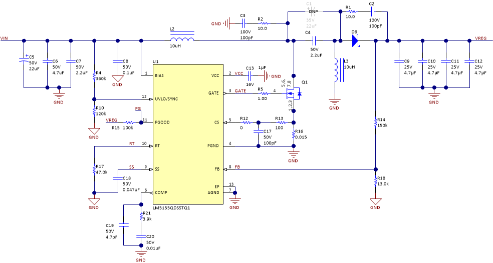
Figure 2-7 shows the default schematic of LM5155-Q1 in SEPIC configuration of this reference design.
 Figure 2-7 Schematic of LM5155-Q1 Controller (SEPIC Configuration)
The main components in the schematic are selected by following the guidelines in the LM5155x-Q1 2.2-MHz Wide Input Non-synchronous Boost/Sepic/Flyback Controller data sheet.
Input capacitors C5, C6, C7 and C8 smooth the input voltage ripple and provide a low impedance supply. The voltage divider resistors R4 and R10 set the desired startup and shutdown voltage level. For this reference design, the startup voltage is 6 V with a hysteresis of 2 V, which results in a 4-V shutdown voltage. Resistor R17 and capacitor C18 are used to set the switching frequency and softstart time. For compensation of the voltage regulator loop C19, R21 and C20 are connected to the comp pin which is the output of the internal transconductance error amplifier. Resistors R14 and R18 adjust the output voltage level. For the internal VCC regulator which supplies the gate driver C13 is required as bypass capacitor. Resistor R13 and capacitor C17 set the slope compensation. A resistor-capacitor snubber network (R2, C3) across the low-side N-channel MOSFET Q1 and (R1, C2) across the requtifier diode reduces ringing and spikes at the switch nodes. For how to calculate these values, see Power Tips: Calculate an R-C snubber in seven steps.
The output capacitors C9, C10, C11 and C12 smooth the output voltage ripple and provide a source of charge during transient loading conditions. The output capacitors also reduce the output voltage overshoot when the load is disconnected suddenly. In a SEPIC regulator, the output is supplied by discontinuous current and the ripple current requirement is usually high, which makes ceramic capacitors a perfect fit. The output voltage ripple is dominated by ESR of the output capacitors. Paralleling the output capacitor is a good choice to minimize effective ESR and split the output ripple current into capacitors. This example uses four 4.7-µF ceramic capacitors with a voltage rating of 25 V. A higher output voltage ripple in this reference design is not a concern for the linear LED drivers, which are connected to the SEPIC output voltage.
The inductors L2 and L3 have a value of 10 µH with a saturation current rating above the maximum expected inductor current of 2 A at a minimum input voltage of 6 V. C4, with a value of 2.2µF, forms the coupling capacitor and D6 the rectifier diode of the SEPIC. The low-side power switch Q1 is a 60-V rated N-channel MOSFETs in a PowerPAK® package. R16 is the current sense resistor to set the current limit.