TIDUEO0C July 2019 – March 2021
- Description
- Resources
- Features
- Applications
- 5
- 1System Description
-
2System Overview
- 2.1 Block Diagram
- 2.2 Design Considerations
- 2.3
Highlighted Products
- 2.3.1 TPS63900: 1.8V-5.5 VIN Buck-Boost Converter With 75-nA Ultra-low Quiescent Current and 400-mA Output Current
- 2.3.2 TPS610995: 0.7 VIN Synchronous Boost Converter With 400-nA Ultra-low Quiescent Current and 1-A Peak Current
- 2.3.3 TPS62840: 750-mA Synchronous Step-Down Converter With Ultra-low Quiescent Current Consumption
- 2.4 System Design Theory
- 3Hardware, Software, Testing Requirements, and Test Results
- 4Design Files
- 5Software Files
- 6Related Documentation
- 7Terminology
- 8About the Author
- 9Revision History
3.2.2.1 Test Results With the TPS62840 Buck Converter
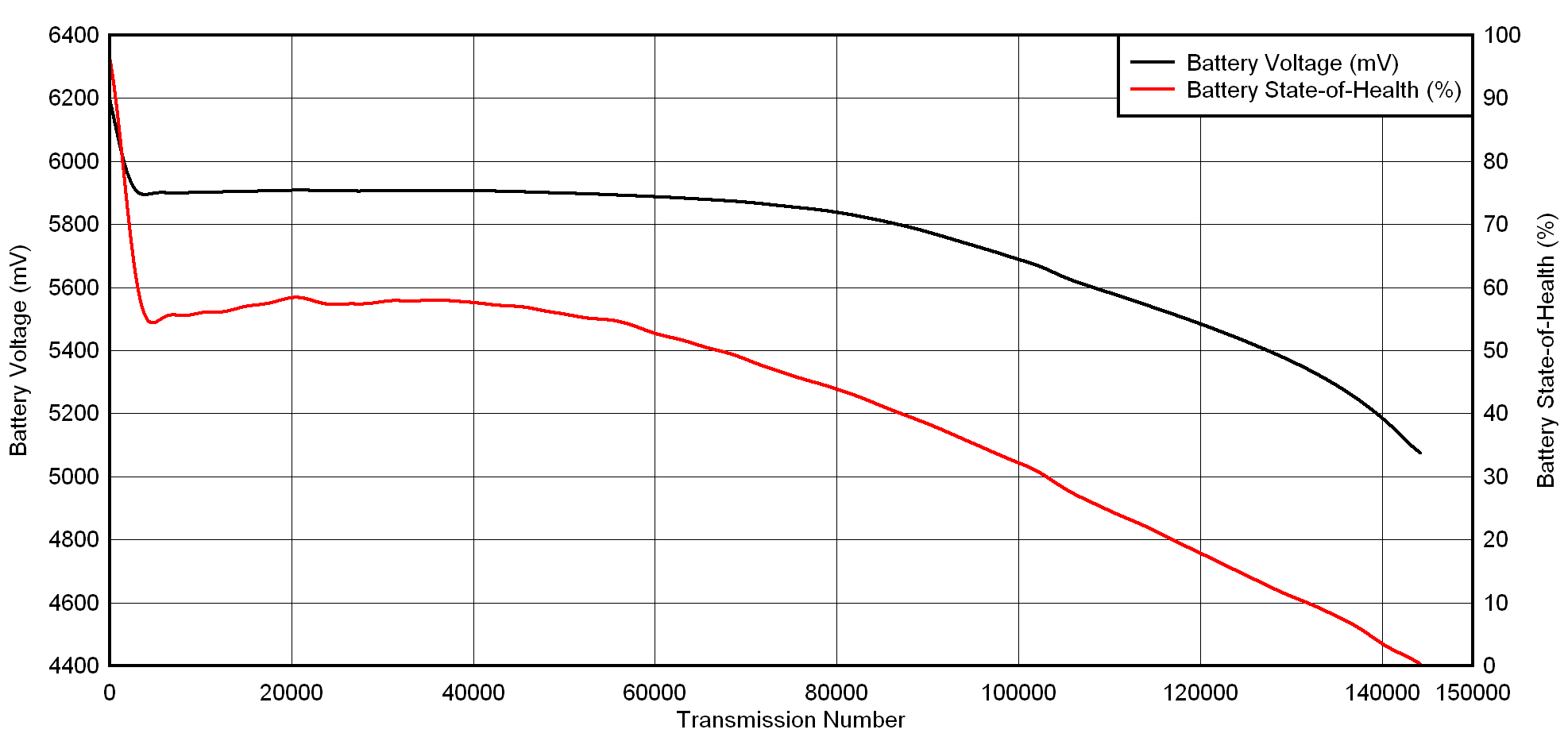
 Figure 3-9 TPS62840 Buck Battery Discharge Data (2s Configuration)
In this figure and all the subsequent transmission figures, it is assumed that the batteries operating range is from 100% SOH to 10% SOH. The 10% SOH cutoff will be used to compare the three different power topologies. Figure 3-9 shows that the cells can withstand approximately 135,000 transmissions (taken at 10% SOH), using the TPS62840 buck converter to power NB-IoT modules. It is important to acknowledge that this test was conducted over a short period of time, where in the field, stand-by current will play a factor in addition to the 250-mA pulses. This will be taken into account in Section 3.2.2.4, where real world battery lifetime estimations are made for the different topologies.
Since the LiMn02 battery chemistry very strongly maintains its voltage, partially increasing for the first half of its lifetime, the gauge will return a more coarse measurement surrounding SOH. However, around the midpoint at 70,000 transmissions, SOH approaches 50% and eventually drops to 0% consistently. See the FDK CR17500EP LiMnO2 primary battery data sheet to observe typical voltage discharge curves.
It is important to note the market leading light-load efficiency of the TPS62840 buck converter at 10 µA (the stand-by current in this test) (see Efficiency vs. Load Current plot in the TPS62840 1.8-V to 6.5-V, 750-mA, 60-nA IQ Step-Down Converter Data Sheet. The efficiency is in the range of 82–88% for VIN = 6.5 V to VIN = 4.2 V (representing fully charged and almost fully discharged two in-series cells) for VOUT = 1.8 V.
In this test, the TPS62840 device operates at VOUT = 3.3 V to power the NB-IoT modules. With a smaller voltage level difference between VIN and VOUT, it will deliver several percent points higher efficiency numbers than those in the data sheet plot.