TIDUEZ8C december 2022 – june 2023
2.3.2.1 Differential to Single-Ended Conversion
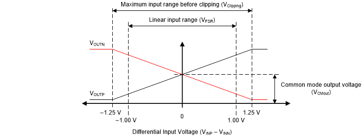
As stated, the isolation voltage is monitored with an AMC3330 across the isolation barrier. The output of the AMC3330 is a fully-differential analog signal comprised of the OUTP and OUTN pins centered around a common-mode voltage of 1.44 V that can be fed directly to a stand-alone analog-to-digital converter (ADC).

Figure 2-9 AMC3330 Output Behavior
The MSP430 and C2000 family of processors have embedded single-ended input ADCs. The addition of a differential to single-ended amplifier output stage, illustrated in Figure 2-10, allows the full output range of the AMC3330 to be converted to the 3.3-V range which is designed for the single-ended embedded ADC. The signal range is amplified, and the common-mode voltage is set to half of the ADC range using 1.65 V provided by REF2033.

Figure 2-10 Differential to Single-Ended Conversion – Output AMC3330
If R1 = R4 and R2 = R3 Equation 19 describes the behavior of the differential-to-single-ended conversion.
The TLV6001 operational amplifier for cost-sensitive systems is used for this purpose. Further details on the TI isolated amplifier family differential output conversion to singled ended are found in the Interfacing a Differential-Output (Isolated) Amplifier to a Single-Ended Input ADC application brief.
The AMC3330 has a maximum output voltage swing of ±2 V. This has to be translated to a single-ended signal between 0 V and 3.3 V. Hence, a gain of 0.825 is set with the ratio of R1/R2 and R4/R3. The common-mode voltage of 1.65 V is set with the Vref / 2 output of the REF2033 voltage reference.