TIDUEZ8C december   2022  – june 2023


  1.   1
  2.   Description
  3.   Resources
  4.   Features
  5.   Applications
  6.   6
  7. 1System Description
    1. 1.1 Insulation Monitoring
    2. 1.2 Impact of Parasitic Isolation Capacitance
    3. 1.3 IEC 61557-8 Standard for Industrial Low-Voltage Distribution Systems
    4. 1.4 Key System Specifications
  8. 2System Overview
    1. 2.1 Block Diagram
    2. 2.2 Highlighted Products
      1. 2.2.1 TPSI2140
      2. 2.2.2 AMC3330
      3. 2.2.3 TPS7A24
      4. 2.2.4 REF2033
      5. 2.2.5 TLV6001
    3. 2.3 Design Considerations
      1. 2.3.1 Resistive Bridge
      2. 2.3.2 Isolated Analog Signal Chain
        1. 2.3.2.1 Differential to Single-Ended Conversion
        2. 2.3.2.2 High-Voltage Measurement
        3. 2.3.2.3 Signal Chain Error Analysis
      3. 2.3.3 Loss of PE Detection
      4. 2.3.4 Insulation Monitoring on AC Lines
      5. 2.3.5 PCB Layout Recommendations
  9. 3Hardware, Software, Testing Requirements, and Test Results
    1. 3.1 Hardware Requirements
      1. 3.1.1 Connectors
      2. 3.1.2 Default Jumper Configuration
      3. 3.1.3 Prerequisites
    2. 3.2 Software Requirements
    3. 3.3 Software
    4. 3.4 Test Setup
    5. 3.5 Test Results
  10. 4Design and Documentation Support
    1. 4.1 Design Files
      1. 4.1.1 Schematics
      2. 4.1.2 BOM
    2. 4.2 Documentation Support
    3. 4.3 Support Resources
    4. 4.4 Trademarks
  11. 5About the Author
  12. 6Revision History

PCB Layout Recommendations

The PCB layout for isolation leakage current measurements must be based on the requirements and components selected for the design.

  • The high-voltage section of the system must not have any polygons to HV positive, HV negative, or PE.
  • Maintain creepage and clearance distances required for isolation between the HV positive, HV negative, and PE.
  • Place thin film resistors in series or a series parallel combination that maintains the isolation and does not allow any low-ohmic paths due to PCB, humidity, or liquids, which are all probable occurrences on the PCB.
  • Maintain creepage and clearance distances required for isolation components (AMC3330 and TPSI2140) as explained in the device data sheet.
  • To minimize noise, take care when placing analog lines to avoid noise from relays and power switching components.
  • Follow the component data sheet to minimize the EMC issues on layout.

Figure 2-15 shows the PCB layout recommendations.
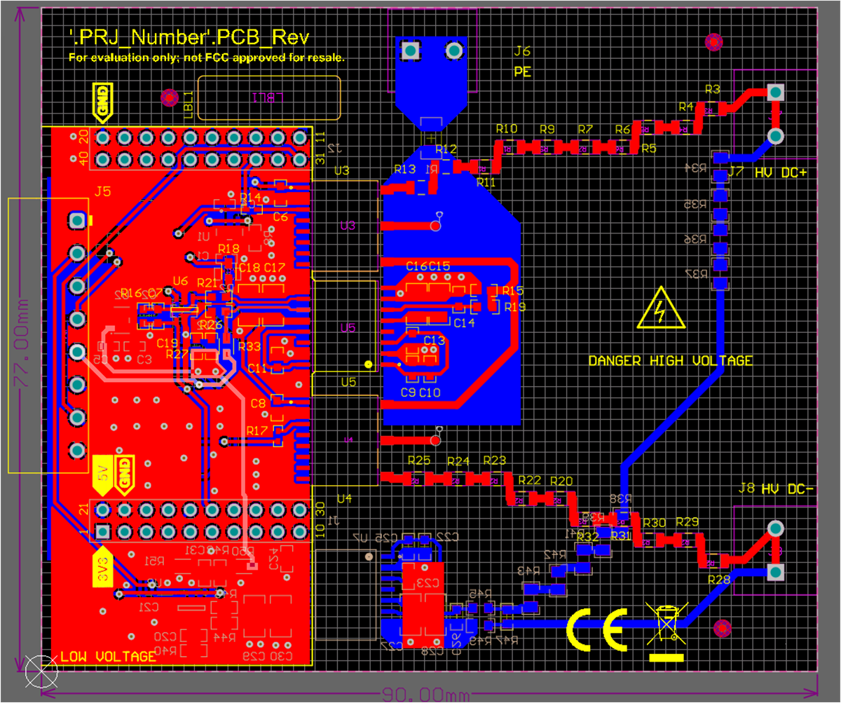
GUID-20220401-SS0I-RDHW-8L5S-8CGHTGXGMVRS-low.pngFigure 2-15 Layout Recommendations - Creepage