TIDUEZ8C december   2022  – june 2023


  1.   1
  2.   Description
  3.   Resources
  4.   Features
  5.   Applications
  6.   6
  7. 1System Description
    1. 1.1 Insulation Monitoring
    2. 1.2 Impact of Parasitic Isolation Capacitance
    3. 1.3 IEC 61557-8 Standard for Industrial Low-Voltage Distribution Systems
    4. 1.4 Key System Specifications
  8. 2System Overview
    1. 2.1 Block Diagram
    2. 2.2 Highlighted Products
      1. 2.2.1 TPSI2140
      2. 2.2.2 AMC3330
      3. 2.2.3 TPS7A24
      4. 2.2.4 REF2033
      5. 2.2.5 TLV6001
    3. 2.3 Design Considerations
      1. 2.3.1 Resistive Bridge
      2. 2.3.2 Isolated Analog Signal Chain
        1. 2.3.2.1 Differential to Single-Ended Conversion
        2. 2.3.2.2 High-Voltage Measurement
        3. 2.3.2.3 Signal Chain Error Analysis
      3. 2.3.3 Loss of PE Detection
      4. 2.3.4 Insulation Monitoring on AC Lines
      5. 2.3.5 PCB Layout Recommendations
  9. 3Hardware, Software, Testing Requirements, and Test Results
    1. 3.1 Hardware Requirements
      1. 3.1.1 Connectors
      2. 3.1.2 Default Jumper Configuration
      3. 3.1.3 Prerequisites
    2. 3.2 Software Requirements
    3. 3.3 Software
    4. 3.4 Test Setup
    5. 3.5 Test Results
  10. 4Design and Documentation Support
    1. 4.1 Design Files
      1. 4.1.1 Schematics
      2. 4.1.2 BOM
    2. 4.2 Documentation Support
    3. 4.3 Support Resources
    4. 4.4 Trademarks
  11. 5About the Author
  12. 6Revision History

AMC3330

The AMC3330 is a fully-differential precision isolated amplifier with high-input impedance, and an integrated DC/DC converter that allows the device to be supplied from a single 3.3-V or 5-V voltage supply source from the low voltage side. The input stage of the device drives a 2nd-order, delta-sigma (ΔΣ) modulator. The modulator uses an internal voltage reference and clock generator to convert the analog input signal to a digital bitstream. The drivers (termed TX in the Functional Block Diagram) transfer the output of the modulator across the isolation barrier that separates the high-side and low-side voltage domains. The received bitstream and clock are synchronized and processed by a 4th-order analog filter on the low-side and presented as a differential analog output.

Figure 2-3 shows the AMC3330 block diagram. The 1.2-GΩ differential input impedance of the analog input stage supports low gain-error signal-sensing in high-voltage applications using high-impedance resistor dividers. The signal path is isolated by a double capacitive silicon-dioxide (SiO 2) insulation barrier, whereas power isolation uses an on-chip transformer separated by a thin-film polymer as the insulating material.
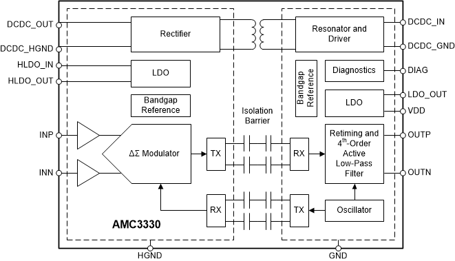
GUID-37695D9F-95E9-4A86-B3D4-D9732E1EF778-low.gif Figure 2-3 AMC3330 Functional Block Diagram