SBAA542 March 2022 AMC23C10
Design Goals
| High Side Supply | Input Voltage |
Working Voltage |
Low Side Supply |
Output Voltage |
|---|---|---|---|---|
12 V | ±170 Vpk Sine Wave | ≥ 400 VRMS | 3.3 V to 5.0 V ±10% | ≤ Low-Side Supply |
Design Description
A zero-crossing detector circuit changes output state when the AC input crosses the zero-cross reference voltage. This design features a single chip solution for zero-crossing detection of an AC sine wave with inverting and non-inverting digital outputs. The circuit is created by setting the comparator inverting input to ground and applying a clamped sine wave to the noninverting input. The input voltage is clamped by R1 and a pair of antiparallel diodes. In this case, diodes are used instead of an attenuator to maximize the slew rate of the input near the zero-crossing, which reduces output latency. The circuit is used for AC line zero-cross detection in control circuits to reduce standby and off-mode power consumption.
Design Notes
- The circuit must be capable of handling 750-V working voltage across the isolation barrier.
- The maximum input voltage at IN+ must be ±1 V
- Inverting and non-inverting output are desired
- Maximum current flowing through R1 is 100 µA ±10%
- Limit the operating voltage of each resistor in the string to 100 V ±10% maximum
- The input AC source voltage is 120 VRMS, higher AC voltages are easily accommodated with component modifications. See the Alternate Design section for details
- Ensure the hysteresis voltage at the AC zero-cross is no more than ±30 mV
Design Steps
- Determine the ideal R1 resistor value. The
maximum peak input voltage of 120 VRMS × √2 = 170 VPK.
Note that the forward voltage of the diode D1 is near zero, and not included in
this calculation.
- Divide R1 into 3 equal resistors to maintain design limits of ≤ 100 V per resistor:
- Use the Analog Engineer’s Calculator to find a standard E96 1% resistor value for R1. The nearest value is 569 kΩ.
- Select the anti-parallel diodes. Choose diodes which will provide at least ± 350-mV forward voltage with the 100 µA supplied through R1.
- Optional – design low-pass filter at VINP defined
by R2 and C1. The frequency response is defined as:
Revised Design
The following schematic shows implementation of the revised design using the AMC23C10.
The AMC23C10 uses capacitive isolation to provide a working voltage of 1000 V. The voltage source for VDD1 is specified from 3 V to 27 V, controlled internally through an LDO. VDD2 is specified from 2.7 V to 5.5 V. The input voltage range under normal operation is ±1 V. The logic output on OUT1 is open drain which can be used with a pullup resistor to VDD1. OUT2 is a push-pull type output needing no external pullup resistors.
Design Simulations
Measured Response
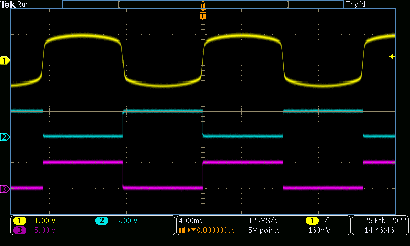
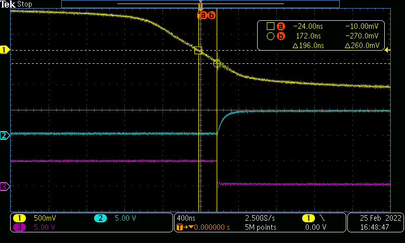
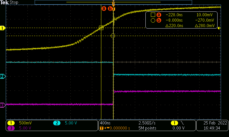
The following images show the measured response of the zero-crossing detection circuit using the AMC23C10 isolated comparator. The input is captured on trace 1, while OUT1 and OUT2 are shown on traces 2 and 3 respectively. When measured at both the rising and falling edges of the input, the delay between the zero-crossing of the input and the output transition does not exceed 220 ns.
 Zero-Crossing Detection of Rectified Input
 Zero-Crossing Detection Output Latency – Falling Edge
 Zero-Crossing Detection Output
Latency – Rising Edge
Zero-Crossing Detection Output
Latency – Rising EdgeDesign References
See Analog Engineer's Circuit Cookbooks for TI's comprehensive circuit library.
Texas Instruments, AMC23C10 Fast Response, Reinforced Isolated Comparator With Dual Output data sheet
Design Featured Isolated Comparator
| AMC23C10 | |
|---|---|
| Working Voltage | 1000 VRMS |
| VDD1 | 3.0 V–27 V |
| VDD2 | 2.7 V–5.5 V |
| Input Voltage Range | ±1000 mV |
| Output Options | OUT1 - Open Drain |
| OUT2 - Push-Pull | |
| AMC23C10 | |
Alternate Design for 230-VAC Input
| AMC23C10 | |
|---|---|
| Working Voltage | 1000 VRMS |
| AC Input | 325 Vpk |
| R1 Ideal | 3.25 MΩ |
| R1 E96 Standard | Three each 1.09 MΩ |