SBOA258A February 2019 – December 2020 OPA322 , OPA354 , OPA620
Design Goals
| Input | Output | Bandwidth | Supply | ||||
|---|---|---|---|---|---|---|---|
| ViMin | ViMax | VoMin | VoMax | BW | Vcc | Vee | Vref |
| –0.24V | +0.24V | +0.1V | +4.9V | 10MHz | +2.5V | 0V | 2.5V |
Design Description
This design uses 3 op–amps to build a discrete wide bandwidth instrumentation amplifier. The circuit converts a differential, high frequency signal to a single–ended output.
Design Notes
- Reduce the capacitance on the output of each op amp to avoid stability issues.
- Use low gain configurations to maximize the bandwidth of the circuit.
- Use precision resistors to achieve high DC CMRR performance.
- Use small resistors in op–amp feedback to maintain stability.
- Set the reference voltage, Vref, at mid–supply to allow the output to swing to both supply rails.
- Phase margin of 45° or greater is required for stable operation.
- R7 sets the gain of the instrumentation amplifier.
- Linear operation depends upon the input common–mode and the output swing ranges of the discrete op amps used. The linear output swing ranges are specified under the Aol test conditions in the op amps datasheets.
- Vref also sets the common-mode voltage of the input, Vi, to ensure linear operation.
Design Steps
- The transfer function of the circuit is given below. Equation 1.

where Vi is the differential input voltage
Vref is the reference voltage provided to the amplifier
Equation 1.
- To maximize the usable bandwidth of design, set the gain of the diff amp stage to 1V/V. Use smaller value resistors to minimize noise.
Equation 1.
- Choose values for resistors R1 and R2. Keep these values low to minimize noise.
Equation 1.
- Calculate resistor R7 to set the gain of
the circuit to 10V/V Equation 1.
 Equation 1.
- Calculate the reference voltage to bias the input to mid-supply. This will maximize the linear output swing of the instrumentation amplifier. See References for more information on the linear operating region of instrumentation amplifiers.
Equation 1.
Design Simulations
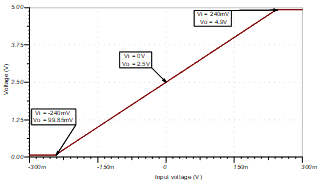
DC Simulation Results
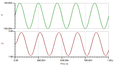
Transient Simulation Results
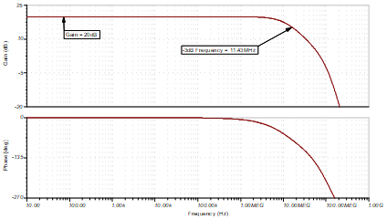
AC Simulation Results
References
- Analog Engineer's Circuit Cookbooks
- SPICE Simulation File SBOMAU6
- TI Precision Labs
- Instrumentation Amplifier VCM vs. VOUT Plots
- Common-mode Range Calculator for Instrumentation Amplifiers
| OPA354 | |
|---|---|
| Vss | 2.5V to 5.5V |
| VinCM | Rail–to–rail |
| Vout | Rail–to–rail |
| Vos | 2mV |
| Iq | 4.9mA/Ch |
| Ib | 3pA |
| UGBW | 250MHz |
| SR | 150V/µs |
| #Channels | 1,2,4 |
| www.ti.com/product/opa354 | |
Design Alternate Op Amp
| OPA322 | |
|---|---|
| Vss | 1.8V to 5.5V |
| VinCM | Rail–to–rail |
| Vout | Rail–to–rail |
| Vos | 500µV |
| Iq | 1.6mA/Ch |
| Ib | 0.2pA |
| UGBW | 20MHz |
| SR | 10V/µs |
| #Channels | 1,2,4 |
| www.ti.com/product/opa322 | |
Revision History
| Revision | Date | Change |
|---|---|---|
| A | December 2020 | Updated R11 to R7 for resistor number consistency |