SBOA270C March 2019 – December 2020 LMV358 , TLV170
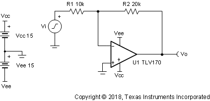
Design Goals
| Input | Output | Freq. | Supply | |||
|---|---|---|---|---|---|---|
| ViMin | ViMax | VoMin | VoMax | f | Vcc | Vee |
| –7V | 7V | –14V | 14V | 3kHz | 15V | –15V |
Design Description
This design inverts the input signal, Vi, and applies a signal gain of –2V/V. The input signal typically comes from a low-impedance source because the input impedance of this circuit is determined by the input resistor, R1. The common-mode voltage of an inverting amplifier is equal to the voltage connected to the non-inverting node, which is ground in this design.
Design Notes
- Use the op amp in a linear operating region. Linear output swing is usually specified under the AOL test conditions. The common-mode voltage in this circuit does not vary with input voltage.
- The input impedance is determined by the input resistor. Make sure this value is large when compared to the source output impedance.
- Using high value resistors can degrade the phase margin of the circuit and introduce additional noise in the circuit.
- Avoid placing capacitive loads directly on the output of the amplifier to minimize stability issues.
- Small-signal bandwidth is determined by the noise gain (or non-inverting gain) and op amp gain-bandwidth product (GBP). Additional filtering can be accomplished by adding a capacitor in parallel to R2. Adding a capacitor in parallel with R2 improves stability of the circuit if high value resistors are used.
- Large signal performance can be limited by slew rate. Therefore, check the maximum output swing versus frequency plot in the data sheet to minimize slew-induced distortion.
- For more information on op amp linear operating region, stability, slew-induced distortion, capacitive load drive, driving ADCs, and bandwidth, see the Design References section.
Design Steps
The transfer function of this circuit follows:
- Determine the starting value of
R1. The relative size of R1 to the signal source
impedance affects the gain error. Assuming the impedance from the signal source
is low (for example, 100Ω), set R1 = 10kΩ for 1% gain error.
Equation 1.
- Calculate the gain required for the
circuit. Since this is an inverting amplifier, use ViMin and
VoMax for the calculation. Equation 1.
- Calculate R2 for a
desired signal gain of –2 V/V. Equation 1.
- Calculate the small signal circuit
bandwidth to ensure it meets the 3-kHz requirement. Be sure to use the noise
gain, or non-inverting gain, of the circuit. Equation 1.Equation 1.Equation 1.
- Calculate the minimum slew rate
required to minimize slew-induced distortion. Equation 1.Equation 1.
- SRTLV170 = 0.4V/µs, therefore, it meets this requirement.
- To avoid stability issues, ensure
that the zero created by the gain setting resistors and input capacitance of the
device is greater than the bandwidth of the circuit. Equation 1.Equation 1.
- Ccm and Cdiff are the common-mode and differential input capacitance of the TLV170, respectively.
- Since the zero frequency is greater than the bandwidth of the circuit, this requirement is met.
Design Simulations
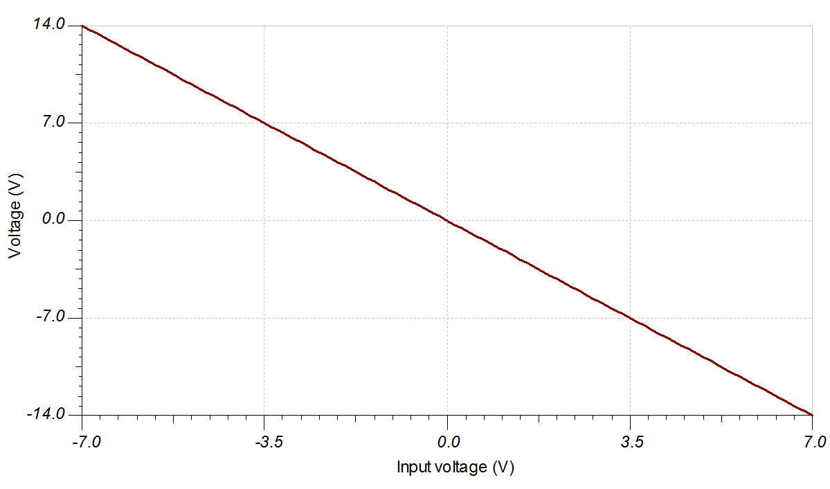
DC Simulation Results
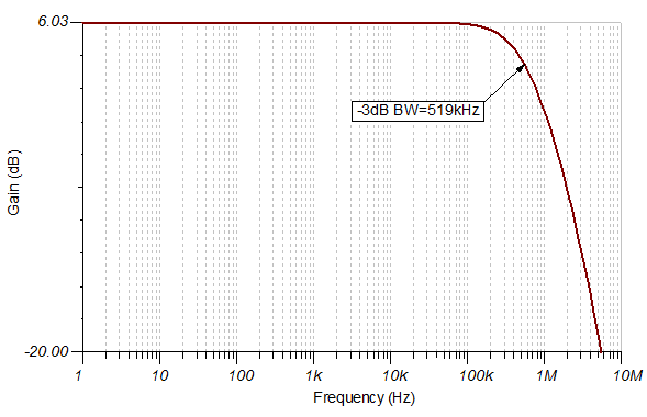
AC Simulation Results
The bandwidth of the circuit depends on the noise gain, which is 3V/V. The bandwidth is determined by looking at the –3-dB point, which is located at 3dB given a signal gain of 6dB. The simulation sufficiently correlates with the calculated value of 400kHz.
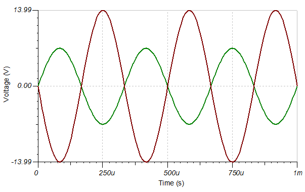
Transient Simulation Results
The output is double the magnitude of the input and inverted.
References:
- Analog Engineer's Circuit Cookbooks
- SPICE Simulation File SBOC492
- TI Precision Labs
Design Featured Op Amp
| TLV170 | |
|---|---|
| Vss | ±18 V (36 V) |
| VinCM | (Vee-0.1 V) to (Vcc-2 V) |
| Vout | Rail-to-rail |
| Vos | 0.5 mV |
| Iq | 125 µA |
| Ib | 10 pA |
| UGBW | 1.2 MHz |
| SR | 0.4 V/µs |
| #Channels | 1, 2, 4 |
| www.ti.com/product/tlv170 | |
Design Alternate Op Amp
| LMV358A | |
|---|---|
| Vss | 2.5 V to 5.5 V |
| VinCM | (Vee–0.1 V) to (Vcc–1 V) |
| Vout | Rail-to-rail |
| Vos | 1 mV |
| Iq | 70 µA |
| Ib | 10 pA |
| UGBW | 1 MHz |
| SR | 1.7 V/µs |
| #Channels | 1 (LMV321A), 2 (LMV358A), 4 (LMV324A) |
| www.ti.com/product/lmv358A | |
| Revision | Date | Change |
|---|---|---|
| C | December 2020 | Updated result for Design Step 6. |
| B | March 2019 | Changed LMV358 to LMV358A in the Design Alternate Op Amp section. |
| A | January 2019 | Downstyle title. Added link to circuit cookbook landing page. |