SBOA282A December 2018 – March 2022 OPA172 , OPA192 , TLV171
Design Goals
| Input Vidiff (Vi2 – Vi1) | Common-Mode Voltage | Output | Supply | ||||
|---|---|---|---|---|---|---|---|
| Vi diff Min | Vi diff Max | Vcm | VoMin | VoMax | Vcc | Vee | Vref |
| -0.5 V | +0.5 V | ±7 V | –5 V | +5 V | +15 V | –15 V | 0 V |
Design Description
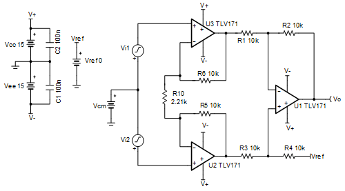
This design uses 3 op amps to build a discrete instrumentation amplifier. The circuit converts a differential signal to a single-ended output signal. Linear operation of an instrumentation amplifier depends upon linear operation of its building block: op amps. An op amp operates linearly when the input and output signals are within the device’s input common-mode and output swing ranges, respectively. The supply voltages used to power the op amps define these ranges.
Design Notes
- Use precision resistors to achieve high DC CMRR performance
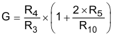
- R10 sets the gain of the circuit.
- Add an isolation resistor to the output stage to drive large capacitive loads.
- High-value resistors can degrade the phase margin of the circuit and introduce additional noise in the circuit.
- Linear operation is contingent upon the input common-mode and the output swing ranges of the discrete op amps used. The linear output swing ranges are specified under the Aol test conditions in the op amps data sheets.
Design Steps
- Transfer function of this circuit:
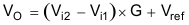
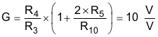
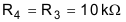
When Vref = 0, the transfer function simplifies to the following equation:
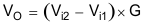
where
- Select the feedback loop resistors
R5 and R6:

- Select R1, R2, R3, R4. To
set the Vref gain at 1 V/V and avoid degrading the instrumentation amplifier's CMRR,
ratios of R4/R3 and R2/R1 must be equal.

- Calculate R10 to meet the
desired gain:

- To check the common-mode voltage range, download and install the program from reference [5]. Edit the INA_Data.txt file in the installation directory by adding the code for a 3 op amp INA whose internal amplifiers have the common-mode range, output swing, and supply voltage range as defined by the amplifier of choice (TLV172, in this case). There is no Vbe shift in this design and the gain of the output stage difference amplifeir is 1 V/V. The default supply voltage and reference voltages are ±15 V and 0 V, respectively. Run the program and set the gain and reference voltage accordingly. The resulting VCM vs. VOUT plot approximates the linear operating region of the discrete INA.
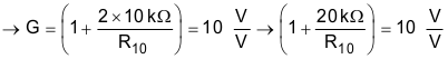
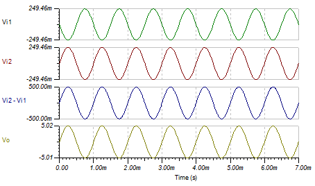
Design Simulations
DC Simulation Results
Transient Simulation Results
References:
- Analog Engineer's Circuit Cookbooks
- SPICE Simulation File SBOMAU8
- TI Precision Labs
- Instrumentation Amplifier VCM vs. VOUT Plots
- Common-mode Range Calculator for Instrumentation Amplifiers
Design Featured Op Amp
| TLV171 | |
|---|---|
| Vss | 4.5 V to 36 V |
| VinCM | (V–) – 0.1 V < Vin < (V+) – 2 V |
| Vout | Rail–to–rail |
| Vos | 0.25 mV |
| Iq | 475 µA |
| Ib | 8 pA |
| UGBW | 3 MHz |
| SR | 1.5 V/µs |
| #Channels | 1,2, and4 |
| TLV171 | |
Design Alternate Op Amp