SBOA547 December 2022 OPA4H199-SEP
1
Design Goals
| Parameter | Value |
|---|---|
| Supply Voltage (Vsupply) | 5 V |
| Input Voltage (Vin) | 0 V to 4.5 V |
| Output Current (Iout) | 0 mA to 90 mA |
| Output Voltage (Vout) | 3.5 V |
| Output Current Error at 90 mA | Circuit 1: <
0.106% Circuit 2: < 0.112% |
| Total Ionizing Dose (TID) | 30-krad (Si) |
| Single Event Latch-up (SEL) Immunity | 43 MeV*cm2/mg |
Design Description
This design generates programmable 90-mA current source to ground. This document shows simulations from two different current sourcing circuits. The simulation results highlight the positives and negatives of each circuit.
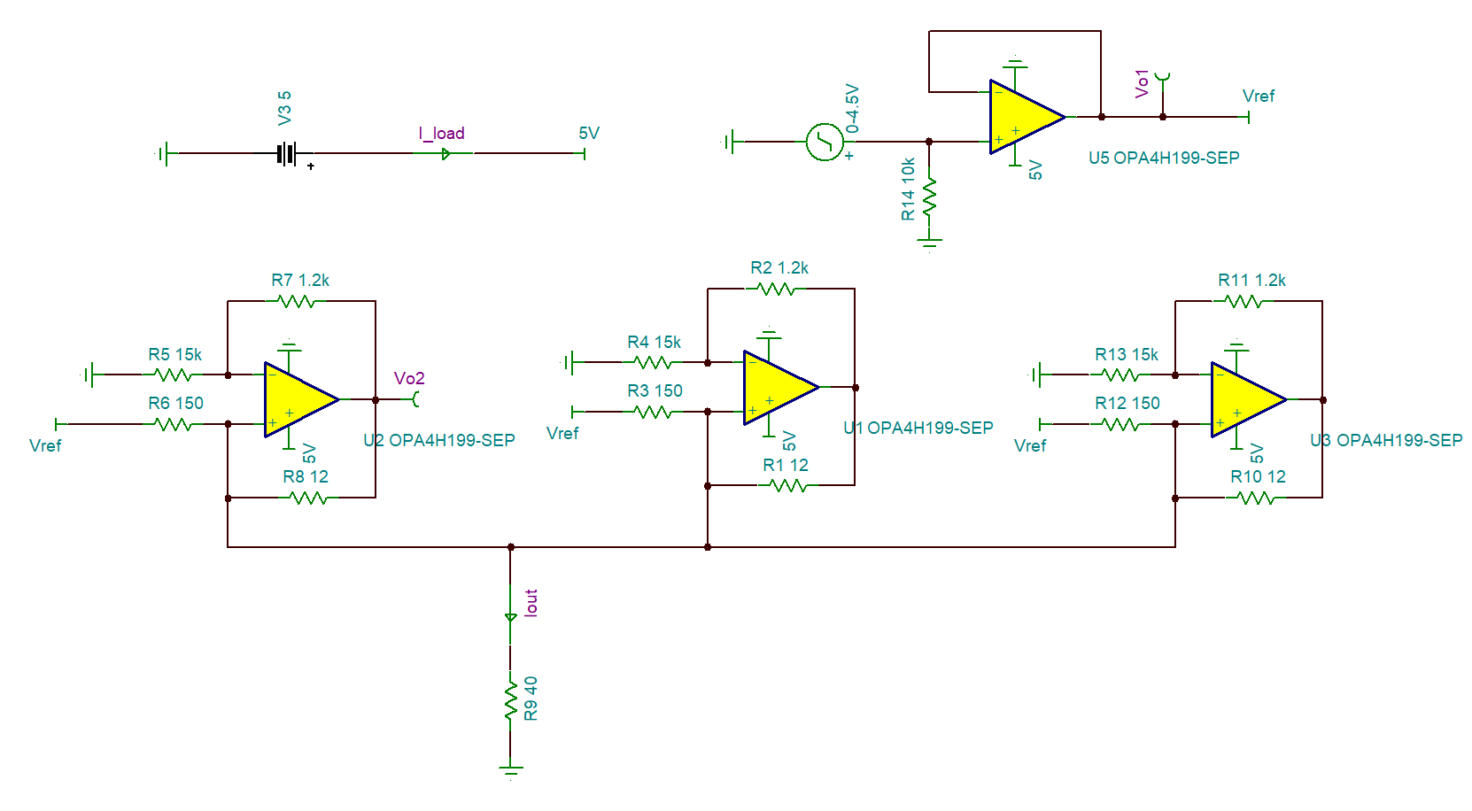
Circuit 1 Schematic shows the first current-sourcing circuit (circuit 1) schematic. In this circuit, each OPA4H199-SEP op amp sources up to 30 mA to support a total of 90 mA current at the load.
 Circuit 1 Schematic
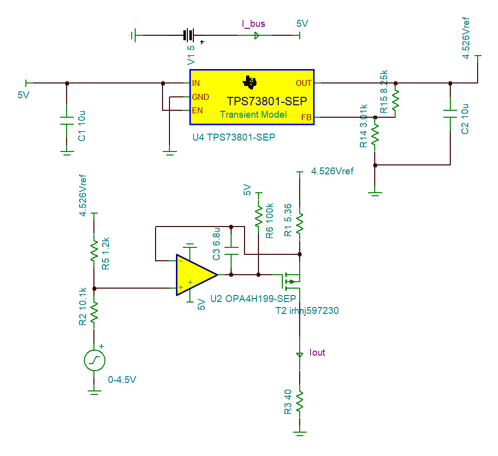
Circuit 2 Schematic shows the second current-sourcing circuit (circuit 2) schematic. In this circuit, the OPA4H199-SEP op amp biases the gate of the PMOS to source 90 mA to the load.
 Circuit 2 Schematic
Design Note
In all simulations, both circuits assume an accurate voltage input for controlling the output current. Both circuits have similar accuracy, but circuit 2 needs calibration to eliminate error causing by the low dropout (LDO).
| Parameter | Circuit 1 | Circuit 2 |
|---|---|---|
| Number of ICs | 1 | 3 |
| Power efficiency at 90 mA | 69.7% | 71% |
| Max error at 90 mA | 0.106% | 0.144% |
| Current sourcing range (mA) | 0 to 90 | 0 to any (depends on PMOS and R1) |
| 3-dB bandwidth (Hz) | 447 | 11.9 kΩ |
Applications
- Radio frequency (RF) front-end biasing
- Temperature sensing
- Battery charging
Design Steps
- Op-amp selection
The OPA4H014 and OPA4H199-SEP devices are considered for use to generate the current source, and their characteristics are put together in the Op-Amp Selection table for comparison.
Op-Amp SelectionDevice # Ch Vs MIN (V) Vs MAX (V) Vos MAX at 25°C (μV) Drift TYP (µV/C) MIN Vcm (V) MAX Vcm (V) IQ typ (mA) Vn (nV/√Hz) IBias (TYP) (nA) OPA4H199-SEP 4 2.7 40 895 0.30 V- – 0.2 V
V+ + 3.2 V 0.56 10.8 0.01 OPA4H014-SEP 4 4.5 18 120 0.35 V-– 0.1 V V+ – 3.5 V 1.8 5.1 0.0005 The OPA4H014-SEP is more precise because this device has a smaller offset voltage (Vos) and drift. However, the upper limit of the common-mode voltage (Vcm) is 3.5 V below the positive supply voltage (V+), which is 5 V – 3.5 V = 1.5 V, in this case. The OPA4H199-SEP, conversely, allows rail-to-rail Vcm, and is selected for circuit 2.
In addition, to configure circuit 1, the op amp must source a large current. The OPA4H014-SEP can source only up to 36 mA when the output is shorted while the OPA4H199-SEP can source up to 75 mA. Hence, OPA4H014-SEP is selected for both circuits.
- LDO selectionNote: Use of LDO in circuit 2 introduces inaccuracy to the system. To eliminate this inaccuracy, a current-sinking circuit instead of sourcing circuit can be configured.
If the 5-V power supply accuracy is not provided, create a reference voltage for circuit 2. Since the Vsupply of the circuit is only 5 V, pick an LDO linear regulator with small dropout voltage (VDO). The LDO selected is the TPS73801-SEP. This LDO has a very small dropout voltage (VDO) of 0.24 V, allowing a maximum reference voltage (Vref) up to 4.76 V with 3% accuracy.
- Resistor selection for circuit 1
and circuit 2
In circuit 1, values of R3, R6, and R12 determine the output current. As an example, consider the left op-amp circuit. This circuit generates a current of Vref / R6, which is 30 mA when Vref is 4.5 V. Since all three op-amp circuits are equivalent, the total output current generated adds up to 90 mA.
In circuit 2, R1 and the voltage across R1 determines the output sourcing current, which is 90 mA when the output current is 0.4824 V. R2 and R5 in the circuit remap the 0-V to 4.5-V input voltage to around 4 V to 4.5 V, such that output current can swing from 0 mA to 90 mA.
- PMOS selection
A MOSFET is used only in circuit 2. The op-amp output is rail to rail and the output ranges from 0 V to 5 V. Hence, the absolute value of the PMOS threshold voltage |Vth| must not be greater than 5 V for the op amp to bias the PMOS gate. The Zero Gate Voltage Drain Current (IDSS) of the PMOS defines the leakage current when the gate voltage is equal to Vbus. IDSS sets the minimum output current.
IRHNJ597230, a 100-krad PMOS is used in circuit 2. As shown in table 4, this IRHNJ597230 has a |Vth| that ranges from 2 – 4 V and a small |IDSS| of 10 – 25 μA.
IRHNJ597230 CharacteristicsIRHNJ597230 D-S Breakdown (V) –200 Vgs (V) –2 to –4 Zero Gate Voltage Drain Current (μA) –10 to –25 Input Capacitance (pF) 1344 Mounting Type SMT Size (mm) 10.28 × 7.64
Circuit 1 Simulation Results
- Error Analysis
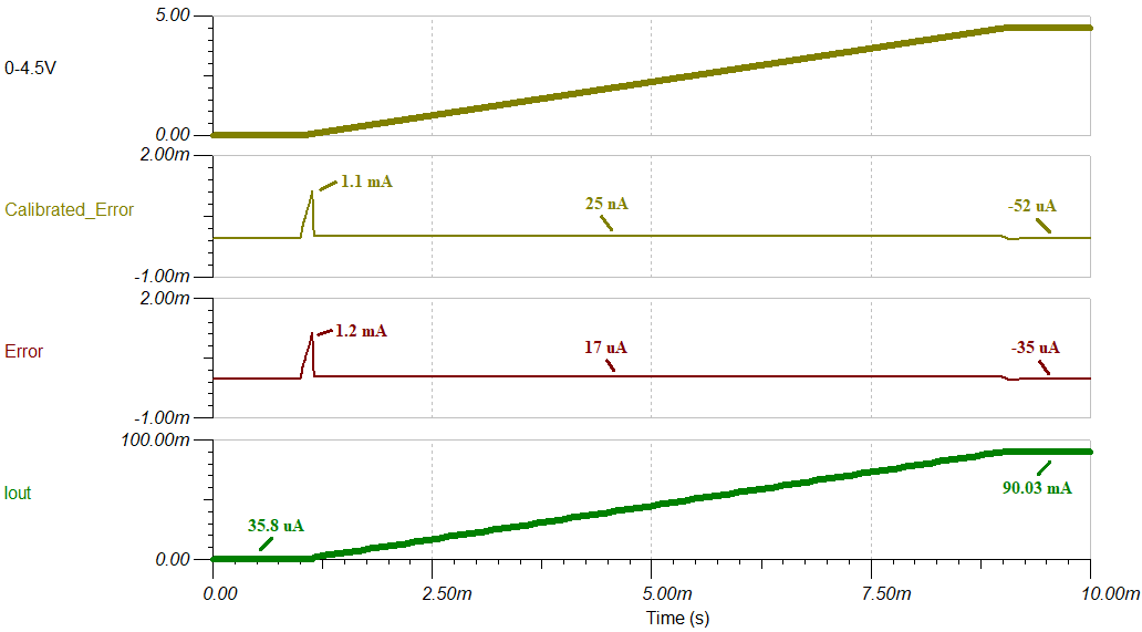
Circuit 1 Simulation Result shows the circuit 1 simulation result. After calibration, the output error is smaller than 52 μA since the input voltage swings from 0 V to 4.5 V. This simulation does not include error caused by the temperature drift of the op-amp offset voltage and resistor tolerance.
 Circuit 1 Simulation Result
The following equations are provided to predict a more accurate percent error.
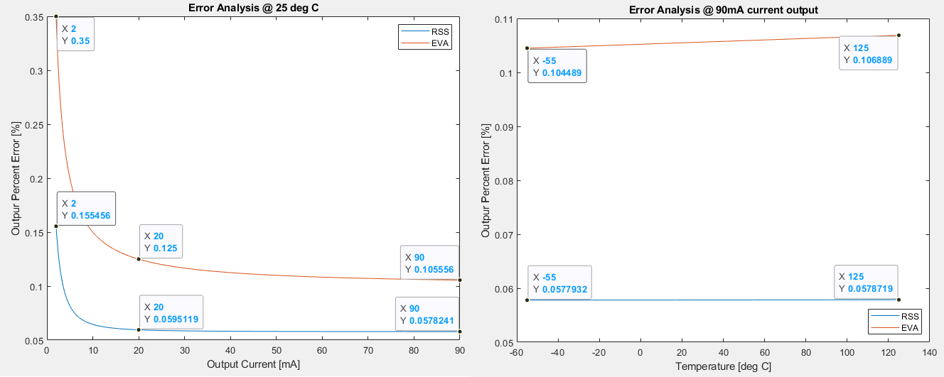
Note: Assume all resistors have 0.1% tolerance. Op-amp offset voltage (Vos) is 125 μV and offset drift (Vos_drift) is 0.3 μV / °C found in the OPA4H199-SEP data sheet.Circuit 1 error analysis is done in MATLAB and shown in Circuit 1 Error Analysis. The first plot shows both RSS and EVA with sourcing current sweeping from 2 mA to 90 mA at 25°C. The second plot shows RSS and EVA with 90-mA sourcing current and temperature sweeping from –55°C to 125°C.
 Circuit 1 Error Analysis
As a conclusion from the two plots in the previous images, accuracy is proportional to the amount of current sourced. Temperature has a very minor effect on accuracy since the offset drift of the op amp is only 0.3 μV / °C. From the results in the images, when sourcing current above 20 mA, the percent error is expected to be smaller than 0.06%.
- Power Consumption
Circuit 1 Power Efficiency shows the circuit 1 power efficiency simulation with input voltage sweeps from 0 to 4.5 V. When the output current is 90 mA, the power consumption reaches the maximum of 465 mW with a power efficiency of 69.7%. When the sourcing current is shut down, the system power consumption is 11.5 mW.
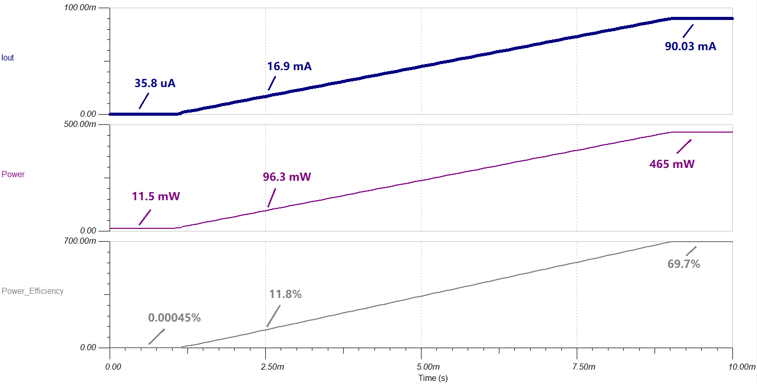 Circuit 1 Power Efficiency
 - Stability Analysis
Circuit 1 Stability Analysis shows the circuit 1 stability analysis simulation result. A small signal transient step response is applied at the op-amp input and percent overshoots are measured at Vo1 and Vo2. Vo1 has 3.89% overshoot, which is equivalent to a 66º phase margin. Vo2 does not have overshoot. Both Vo1 and Vo2 indicate the stability of the system.
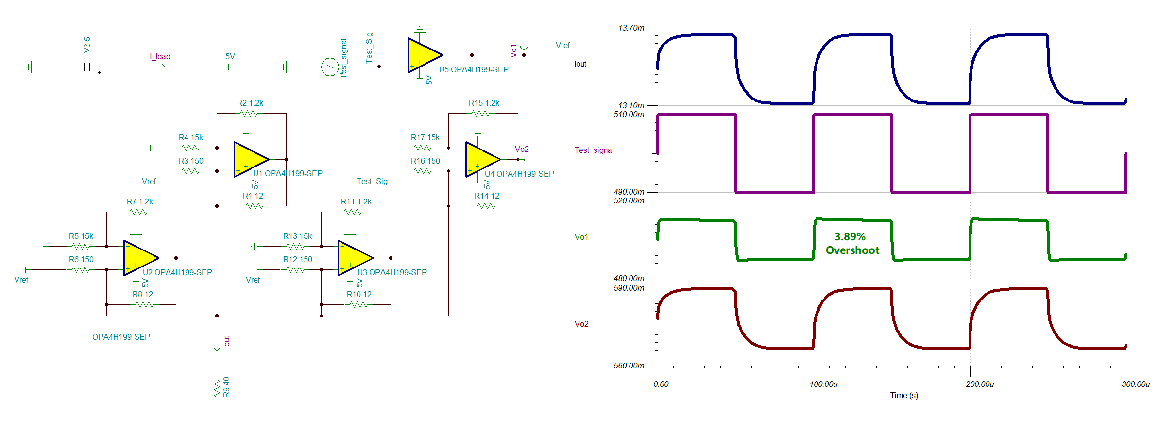 Circuit 1 Stability Analysis
 - Bandwidth
Circuit 1 Bandwidth shows the gain of circuit 1, where Gain = load current / input voltage. The 1% full-power bandwidth and the 3-dB bandwidth are 214 Hz and 447 Hz.
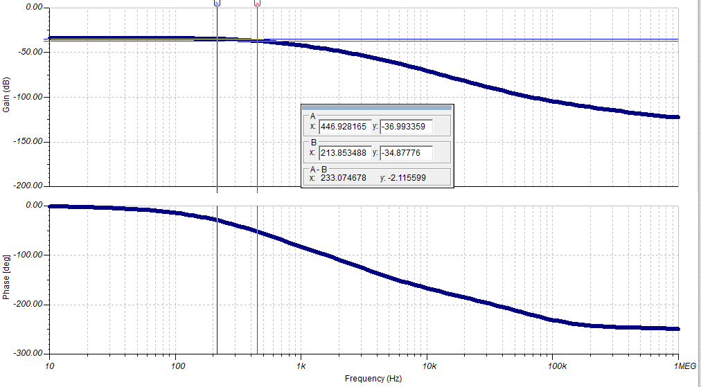 Circuit 1 Bandwidth
Circuit 2 Simulation Results
- Error Analysis
Circuit 2 Simulation Result shows the circuit 2 simulation result. The output current error is smaller than 6.4 μA as input voltage swings from 0 V to 4.5 V. However, this simulation does not include error caused by temperature drift of the op-amp offset voltage and resistor tolerance.
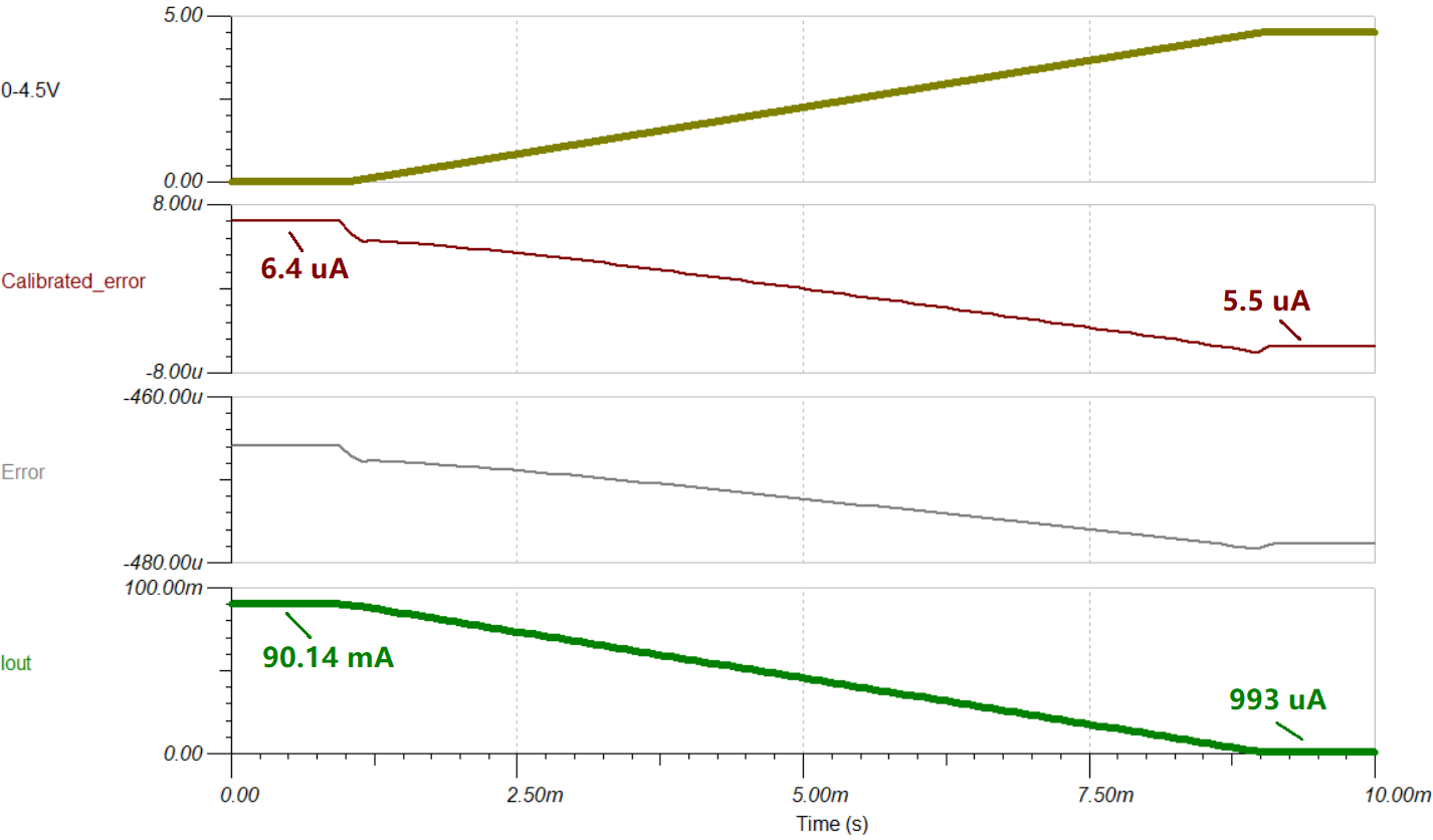 Circuit 2 Simulation Result
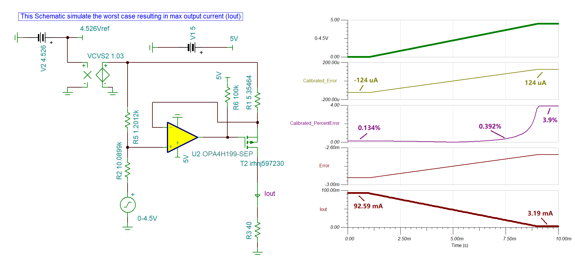
To predict a more accurate percentage error, the worst-case analyses are simulated on TINA spice and shown in Circuit 2 Worst-Case Analysis (Mininum IOUT) and Circuit 2 Worst Case Analysis (Maximum IOUT).
Note: Assume all resistors have 0.1% tolerance. The maximum op-amp offset voltage (Vos) is 830 μV found in the OPA4H199-SEP data sheet. Calibration is done by applying offset to the output result to obtain a 0 error at 45-mA current output.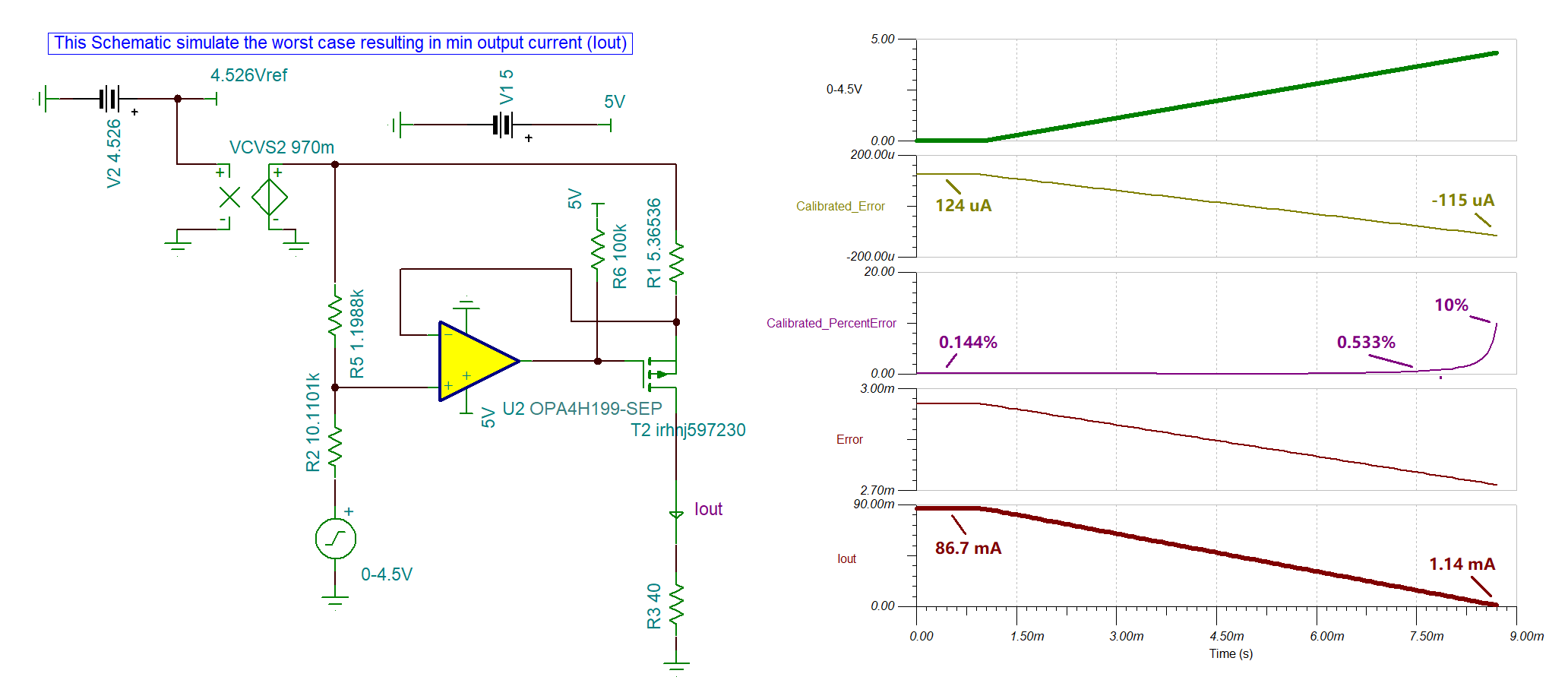 Circuit 2 Worst-Case Analysis (Minimum
IOUT)
Circuit 2 Worst-Case Analysis (Minimum
IOUT)Circuit 2 Worst-Case Analysis (Mininum IOUT) shows the lower end of the maximum current output error. Without calibration, the output current drops down to 86.7 mA at worst case when the output current is supposed to be 90 mA. After calibration, the output error swings from –115 μA to 124 μA. The percent error is 0.144% when sourcing 90 mA to the load, and increases as decreasing sourcing current.
 Circuit 2 Worst-Case Analysis (Maximum
IOUT)
Circuit 2 Worst-Case Analysis (Maximum
IOUT)Circuit 2 Worst-Case Analysis (Maximum IOUT) shows the upper end of the maximum current output error. Without calibration, the output current raises up to 92.59 mA at the worst case when the output current is supposed to be 90 mA. After calibration, the output error swings from –124 μA to 124 μA. The percentage error is 0.134% when sourcing 90 mA to the load, and increases as the sourcing current decreases.
- Power Consumption
Circuit 2 Power Efficiency shows the circuit 2 power efficiency simulation with input voltage sweeps from 0 V to 4.5 V. When the output current is 90 mA, the power consumption reaches the maximum of 458 mW with a power efficiency of 71%. When the sourcing current is shut down, the system power consumption is
10.1 mW.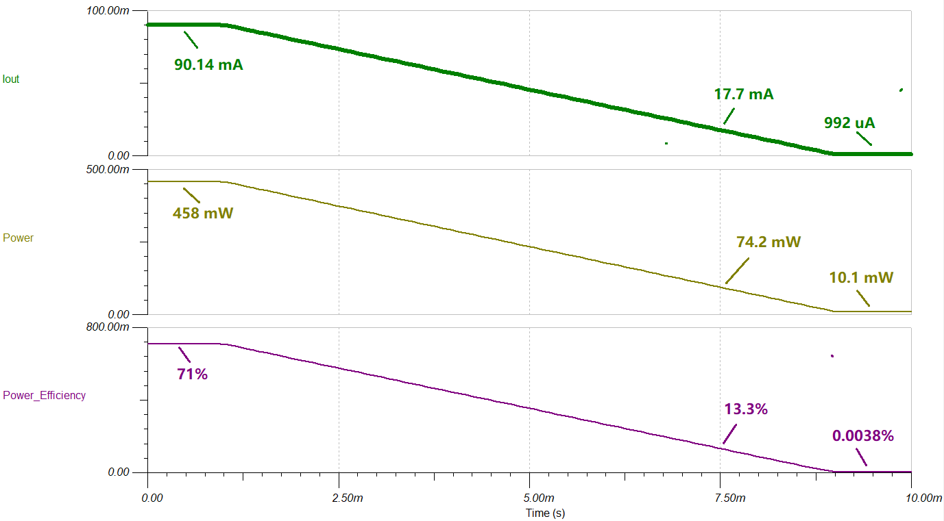 Circuit 2 Power Efficiency
 - Stability Analysis
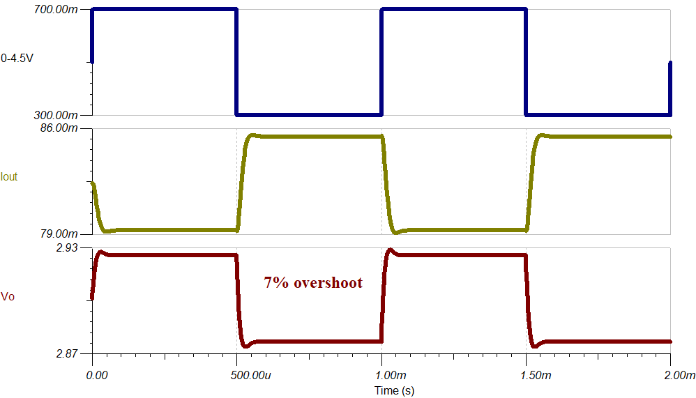
For stability purposes, a 6.8-μF capacitor is placed between the PMOS gate and source. Circuit 2 Stability Analysis shows the stability simulation result done in TINA spice. A small signal transient step response is applied at the op-amp input and percent overshoot is measured at Vo, which is the op-amp output pin as shown in the circuit 2 schematic. Vo has 7% overshoot, which is equivalent to a 62.1º phase margin, indicating the system is stable.
 Circuit 2 Stability Analysis
 - Bandwidth
Circuit 2 Bandwidth is simulated with a 6.8-μF capacitor (C3). This simulation shows the gain of the circuit 2, where Gain = load current / input voltage. The 1% full power bandwidth and the 3-dB bandwidth are 2.26 kHz and 11.9 kHz.
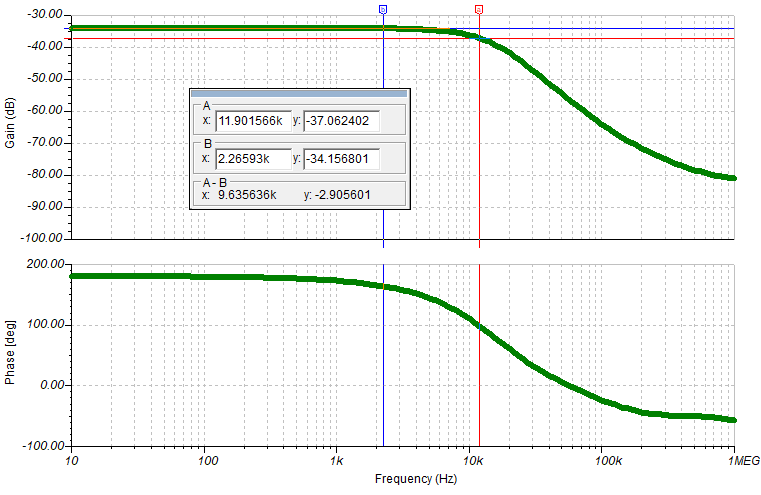 Circuit 2 Bandwidth
Design References
- IR HiRel, “RADIATION HARDENED POWER MOSFET SURFACE MOUNT (SMD-0.5),” IRHNJ597230 data sheet, Dec 2018.
- Texas Instruments, TPS73801-SEP 1-A Low-Noise Fast-Transient-Response Low-Dropout Regulator in Space Enhanced Plastic data sheet