SBVS128F June 2009 – December 2015 TPS727
PRODUCTION DATA.
1 Features
- Very Low Dropout:
- 2% Accuracy Over Load, Line, Temperature
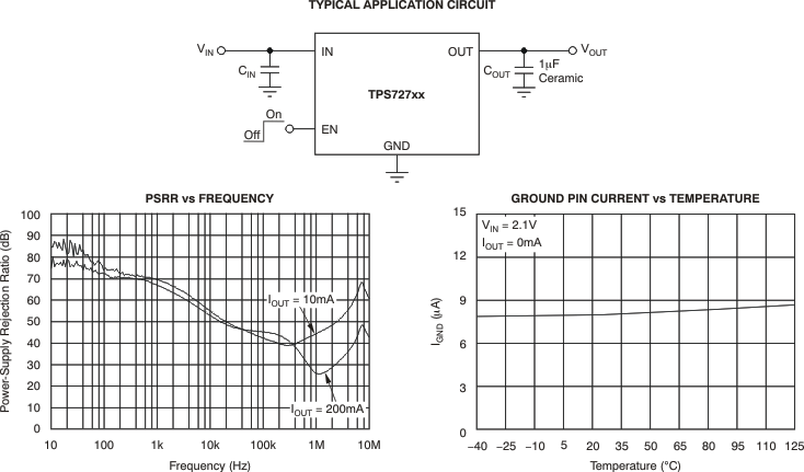
- Ultralow IQ: 7.9 μA
- Excellent Load Transient Performance:±50 mV for 200 mA Loading and Unloading Transient
- Available in Fixed-Output Voltages From 0.9 V to 5 V Using Innovative Factory EEPROM Programming
- High PSRR: 70 dB at 1 kHz
- Stable with a 1.0-μF Ceramic Capacitor
- Thermal Shutdown and Overcurrent Protection
- Available in 4-Ball, 0.4-mm Pitch Wafer-Level Chip Scale and 1.5-mm × 1.5-mm SON Packages
2 Applications
- Wireless Handsets, Smart Phones, PDAs
- MP3 Players and Other Handheld Products
- Wireless LAN, Bluetooth®, Zigbee®
- Remote Controls
- Portable Consumer Products
3 Description
The TPS727 family of low-dropout (LDO) linear regulators are ultralow quiescent current LDOs with excellent line and ultra-fast load transient performance and are designed for power-sensitive applications. The LDO output voltage level is preset by the use of innovative factory EEPROM programming. A precision band-gap and error amplifier provides overall 2% accuracy over load, line, and temperature extremes. The TPS727 family is available in 1.5-mm × 1.5-mm SON and wafer chip-scale (WCSP) packages that make the devices ideal for handheld applications. This family of devices is fully specified over a temperature range of TJ = –40°C to +125°C.
Device Information
| PART NUMBER | PACKAGE | BODY SIZE (NOM) |
|---|---|---|
| TPS727xxDSE | WSON (6) | 1.50 mm × 1.50 mm |
| TPS727xxYFF | DSBGA (4) | 1.20 mm × 0.80 mm |
- For all available packages, see the orderable addendum at the end of the datasheet.

4 Revision History
Changes from E Revision (September 2014) to F Revision
- Changed DSBGA body size in Device Information table Go
Changes from D Revision (February 2014) to E Revision
- Added TPS727105 to documentGo
- Changed terminal to pin throughout documentGo
- Updated Device Information table to current standardsGo
- Changed Pin Configurations note Go
- Changed Pin Functions table: reordered table by pin name, added I/O columnGo
- Updated Handling Ratings table to current standardGo
- Changed Thermal Information table: updated symbolsGo
- Deleted new generation from first sentence of Overview sectionGo
- Added note to Applications and Implementation sectionGo
Changes from C Revision (January, 2011) to D Revision
- Changed format to meet latest data sheet standards; added new sections and moved existing sectionsGo
- Deleted pinout diagrams from front page; see Pin Configurations and Functions section.Go
- Changed Pin Configurations section and moved to Pin Configurations and Functions sectionGo
- Changed note in Pin Configurations and Functions section.Go
- Deleted Figure 26 and Figure 27Go
Changes from B Revision (April, 2010) to C Revision
- Updated YFF front page pin drawing to show pin locationsGo
- Revised Pin Configurations section Go
- Changed graph title for Figure 6Go
Changes from A Revision (September, 2009) to B Revision
- Updated Features listGo
- Changed title of data sheetGo
- Changed footnote 2 to Absolute Maximum Ratings tableGo
- Revised numerous specifications and parameters in Electrical Characteristics tableGo
- Revised operating parameters for Figure 4Go
- Replaced Figure 5Go
- Added operating parameters to Figure 6Go
- Updated Figure 9Go