SLLA553 June 2021 ISOW7740 , ISOW7741 , ISOW7742 , ISOW7743 , ISOW7744
1 Application Brief
As industrial systems trend toward higher voltages, isolation is becoming a requirement for a growing number of systems with multiple power domains. In order for these domains to work together, signal isolation is necessary for signal communication and isolated power is needed to power the secondary side components. Figure 1-1 shows a common block diagram for a group isolated data acquisition system. An isolator is used between the microprocessor (MCU) and analog-to-digital converter (ADC) to protect the MCU from high voltage transients and electrical noise from the field facing input signals. Isolated power is needed to power both the ADC and secondary side of the digital isolator. This example shows a discrete solution that uses a transformer driver, transformer and LDO to power up the ADC and isolator.
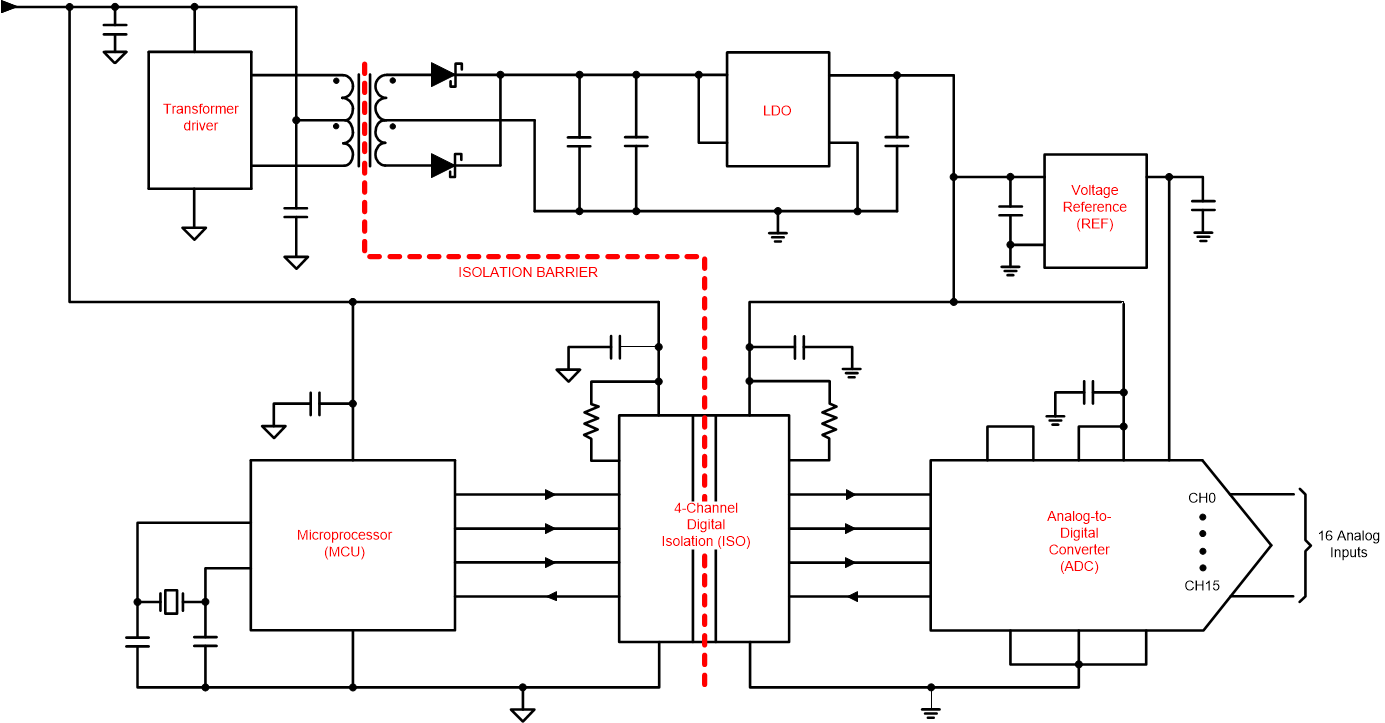 Figure 1-1 Data acquisition system with
discrete isolated power implementation using a transformer driver, transformer, and
LDO
Figure 1-1 Data acquisition system with
discrete isolated power implementation using a transformer driver, transformer, and
LDOWhile a discrete solution can be cost effective, this method can be more complex. It requires various external components consuming a lot of PCB space, especially the external transformer which is bulky and occupies space not only in the X and Y dimension but also in the height.
Conversely, the ISOW7741 reinforced, four-channel digital isolator with integrated chip-scale transformer comes in a single, small-form factor package as shown in Figure 1-2. This device simplifies system design by eliminating the discrete components used in Figure 1-1. ISOW7741 provides up to 30% board space savings, simplicity of design, and reduction of build of materials (BOM).
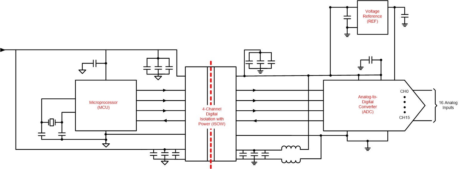 Figure 1-2 Data acquisition system with
integrated isolated power implementation using ISOW7741
Figure 1-2 Data acquisition system with
integrated isolated power implementation using ISOW7741Lower Emissions
ISOW7741 was designed to meet CISPR32 Class B standards with more than 3-dB margin using a cost-effective, two-layer board. TI uses a patented symmetric design architecture in its design and layout of ISOW7741 to provide low emissions. As shown in the internal block diagram of ISOW7741 in Figure 1-3, the VISOIN pin, which powers the digital isolator portion of the circuit, is separated from the VISOOUT pin which is the output of the integrated power converter. This separation of the signal and power path decreases the high-frequency coupling internally inside of the package. Additionally, the switching frequency of the transformer was changed from 60 MHz to 25 MHz to reduce the strength of high frequency components in the emissions spectrum.
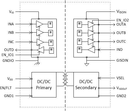 Figure 1-3 Internal block diagram of
ISOW7741 with pin out
Figure 1-3 Internal block diagram of
ISOW7741 with pin outExternal ferrite beads can be used to further attenuate emissions. Placing two 0402 size ferrite beads (Part number: BLM15EX331SN1) on VISOOUT to VISOIN and between the GND2 path, shown in the below figure, will attenuate high frequency noise from the power converter output before that supply line is routed to other components on the PCB. The layout below is recommended to achieve the best performance of the device with optimum efficiency and lowest emissions.
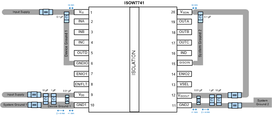 Figure 1-4 ISOW7741 Recommended
Layout
Figure 1-4 ISOW7741 Recommended
LayoutLower Voltage Ripple
The voltage ripple of ISOW7741 was significantly decreased to 24 mV using an adaptive hysteretic controller. Having a low ripple helps with overall system performance around analog circuits as it can alleviate the requirement around their individual power supply rejection ratio (PSRR). A low ripple removes the need for additional filtering using circuitry, such as a LDO, before driving sensitive analog circuits. This saves board space and additional cost of design.
There are two benefits that the adaptive hysteretic controller can provide. First benefit is the increased flexibility of using a decoupling capacitor to further improve the ripple. A voltage ripple of < 10 mV can be achieved with a 100 µF bypass capacitor. The second benefit is that the design has excellent transient load regulation performance, for example, CAN applications where the load changes between 0 and 1.
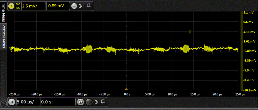 Figure 1-5 ISOW7741 voltage ripple at
less than 3 mVp-p with load > 10%
Figure 1-5 ISOW7741 voltage ripple at
less than 3 mVp-p with load > 10%Additional Diagnostics and Design Enhancements
Diagnostics have also been included in ISOW7741 to verify that the system and product is behaving as expected. The “Enable DC/DC fault protection” pin is used as either an input pin to enable or disable the integrated DC/DC power converter or an output pin, to alert if the power converter is not operating properly. If a fault is reported if VDD > 7 V, VDD < 2.5 V, or if the junction temperature > 170°C, this pin will go low, disabling the DC/DC converter to prevent severe damage of ISOW7741 along with downstream components.
As previously mentioned, the ISOW7741 separates the logic and power paths, which enables a logic supply range of 1.71 V to 5.5 V and a power converter supply range of 3 V to 5.5 V. For example, this allows the power converter to function at 5V in and 5 V out while providing as low as 1.8 V logic to the secondary side component such as an ADC.
ISOW7741 also improves the VISOOUT load regulation from 10% to 5%. Load regulation is important to a system so that a stable voltage supply is provided to the secondary side components as load changes occur. If proper load regulation is not maintained, the downstream devices, such as a transceiver or ADC, will become marginal to their guaranteed values.
ISOW7741 CISPR32 Emissions Data Against Competition
ISOW7741 uses an isolated capacitor combined with an isolated transformer to achieve the industry’s highest isolation ratings and longest lifetime reliability. When controlled power and data signals pass across these isolation barriers, it creates electromagnetic interference (EMI). These radiated emissions (RE) can negatively affect the performance of other electronic systems and networks. Therefore, isolated devices need to maintain electromagnetic compatibility and conform to conducted and radiated emissions standards. The purposes of radiated emission standards/tests are twofold: to ensure that the radiated emissions from a device do not interface with broadcast radio services, and to specify procedures to ensure the reproducibility of measurement and the repeatability of results.
CISPR32 is an electromagnetic compatibility standard for multimedia equipment (MME). This includes information technology equipment (ITE), audio equipment, video equipment, broadcast receiving equipment, and entertainment lighting control equipment. CISPR32 considers two classes of end-user terminal equipment. Class A devices are those that are marketed for use in a commercial, industrial or business environment. Class B devices are those that are marketed for use in the home. Class B limits are more stringent than Class A limits as indicated in the tables below.
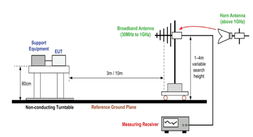 Figure 1-6 CISPR32 test setup
CISPR32 specifies an Equipment Under Test (EUT) placed on a nonconductive turntable in an anechoic chamber as depicted in Figure 6. The EUT is placed 10 meters away from the receiving antenna. The antenna is configured for horizontal and vertical polarizations and adjusted in height between 1 meter and 4 meter. For each antenna height and polarization, the EUT on a turntable is rotated from 0 to 360 degrees to find the maximum field-strength readings. The worst-case emission readings among the different polarizations and heights are recorded from 30 MHz to 1 GHz.
Figure 7 depicts the evaluation module board (EVM) for ISOW7741, used in the CISPR32 radiated emission test. The EVM schematic and PCB layout are available in the ISOW7741DFEVM user guide. Figure 8 shows the high-level block diagram for the ISOW7741 EVM test setup. Ferrite beads are strategically placed, preceding and succeeding the linear regulator (LDO) and at the output power pin (VISOOUT) of the ISO7741 to suppress the system-level emissions. Table 1 shows three configurations for both ISOW7741 and a competitive device that were tested with the CISPR32 Class-B radiated emission standard.
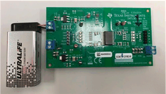 Figure 1-7 ISOW7741 evaluation
module
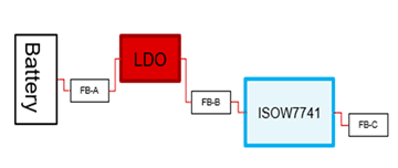 Figure 1-8 ISOW7741 test setup
|
Vcc1 (V) |
Vcc2 (V) |
VISOOUT voltage (V) |
VISOOUT load (mA) |
|
|
Test-1 |
5 |
5 |
5 |
100 |
|
Test-2 |
5 |
3.3 |
3.3 |
50 |
|
Test-3 |
5 |
5 |
5 |
10 |
The below figures show the test results for the three configurations respectively. ISOW7741 passed the CISPR32 Class B radiated emission tests with ample margin for all the three configurations. The competitive device failed the CISPR32 Class B radiated emission tests with 5 V output, 100 mA load (Test 1) and 3.3 V output, 50 mA load (Test 2) configurations. It only passed the 5 V output, 10 mA load (Test 3) test. ISOW7741 not only passed the CISPR32 Class B radiated emission test with sufficient margin but its emission level is independent of the generated output voltage and the amount of load. The consistency of the emission level of ISOW7741 is a significant advantage for a system with variable loading conditions and different voltage levels requirements to meet electromagnetic compatibility (EMC).
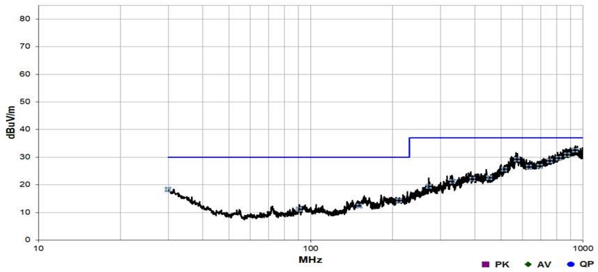 Figure 1-9 ISOW7741 - CISPR32 Class-B
radiated emission results: 5V-input, 5V-output, 100mA-load
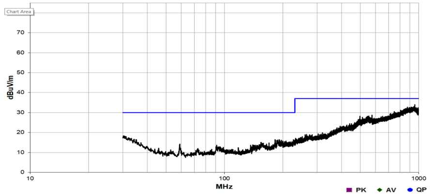 Figure 1-11 ISOW7741 - CISPR32 Class-B
radiated emission results: 5V-input, 3.3V-output, 50mA-load
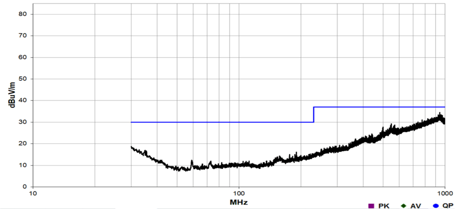 Figure 1-13 ISOW7741 - CISPR32 Class-B
radiated emission results: 5V-input, 5V-output, 10mA-load
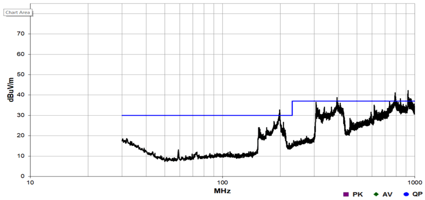 Figure 1-10 Competitive Device -
CISPR32 Class-B radiated emission results: 5V-input, 5V-output,
100mA-load
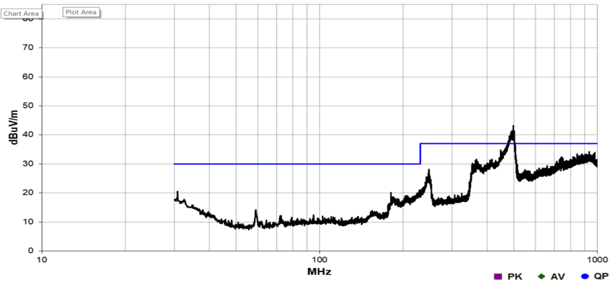 Figure 1-12 Competitor Device -
CISPR32 Class-B radiated emission results: 5V-input, 3.3V-output,
50mA-load
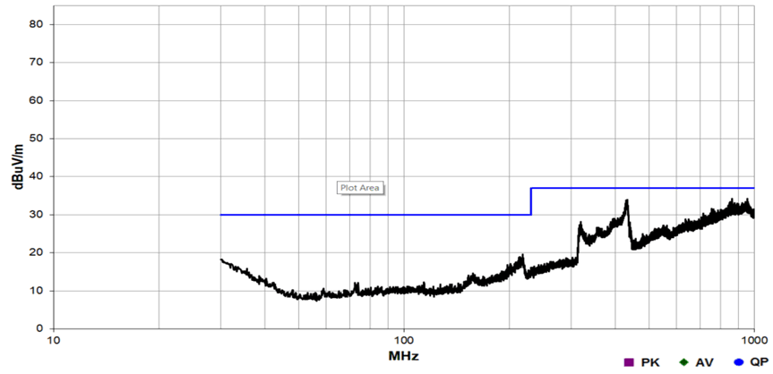 Figure 1-14 Competitor Device -
CISPR32 Class-B radiated emission results: 5V-input, 5V-output,
10mA-load
Figure 1-14 Competitor Device -
CISPR32 Class-B radiated emission results: 5V-input, 5V-output,
10mA-loadFigure 15 shows that using an ISOW7741 in a system designed with good emissions consideration helps keep the emission level as low as the noise floor.
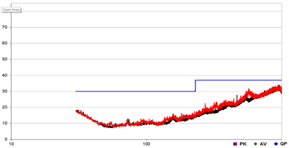 Figure 1-15 Noise floor and ISOW7741
CISPR32 Class-B radiated emission results
Figure 1-15 Noise floor and ISOW7741
CISPR32 Class-B radiated emission resultsConclusion
TI's ISOW7741 provides multiple enhancements while maintaining a small form factor isolated signal and power solution. This device can meet stringent CISPR32 Class B emissions standards using only a two-layer board while remaining agnostic to load conditions and voltage levels. The data against competition proves that ISOW7741 has the lowest emissions in the industry. Improvements in voltage ripple and load regulation confirms a stable integrated power converter and the fault detection pin provides additional security to the user so that the power converters health is closely monitered. All of these features combined help to provide a cost-effective and simple design solution at high performance.