SLLS516E August   2002  – July 2015 SN65LVDS100 , SN65LVDS101 , SN65LVDT100 , SN65LVDT101

UNLESS OTHERWISE NOTED, this document contains PRODUCTION DATA.  

  1. Features
  2. Applications
  3. Description
  4. Revision History
  5. Description (Continued)
  6. Device Options
  7. Pin Configuration and Functions
  8. Specifications
    1. 8.1 Absolute Maximum Ratings
    2. 8.2 ESD Ratings
    3. 8.3 Recommended Operating Conditions
    4. 8.4 Thermal Information
    5. 8.5 Electrical Characteristics
    6. 8.6 Switching Characteristics
    7. 8.7 Typical Characteristics
  9. Parameter Measurement Information
  10. 10Detailed Description
    1. 10.1 Overview
    2. 10.2 Functional Block Diagram
    3. 10.3 Feature Description
      1. 10.3.1 Receiver Features
        1. 10.3.1.1 Voltage Range and Common-Mode Range
        2. 10.3.1.2 Sensitivity
        3. 10.3.1.3 Failsafe Considerations
        4. 10.3.1.4 VBB Voltage Reference
        5. 10.3.1.5 Integrated Termination
        6. 10.3.1.6 Receiver Equivalent Schematic
      2. 10.3.2 Driver Features
        1. 10.3.2.1 Signaling Rate, Edge Rate, and Added Jitter
        2. 10.3.2.2 SN65LVDx100 LVDS Output
          1. 10.3.2.2.1 Driver Output Voltage
          2. 10.3.2.2.2 Driver Offset
        3. 10.3.2.3 SN65LVDx101 LVPECL Output
          1. 10.3.2.3.1 Driver Voltage
        4. 10.3.2.4 Driver Equivalent Schematics
    4. 10.4 Device Functional Modes
  11. 11Application and Implementation
    1. 11.1 Application Information
    2. 11.2 Typical Application
      1. 11.2.1 PECL to LVDS Translation
        1. 11.2.1.1 Design Requirements
        2. 11.2.1.2 Detailed Design Requirements
        3. 11.2.1.3 Application Curve
      2. 11.2.2 LVDS to 3.3-V PECL Translation
        1. 11.2.2.1 Design Requirements
        2. 11.2.2.2 Detailed Design Requirements
        3. 11.2.2.3 Application Curve
      3. 11.2.3 5-V PECL to 3.3-V PECL Translation
        1. 11.2.3.1 Design Requirements
        2. 11.2.3.2 Detailed Design Requirements
        3. 11.2.3.3 Application Curve
      4. 11.2.4 CML to LVDS or 3.3-V PECL Translation
        1. 11.2.4.1 Design Requirements
        2. 11.2.4.2 Detailed Design Requirements
        3. 11.2.4.3 Application Curve
      5. 11.2.5 Single-Ended 3.3-V PECL to LVDS Translation
        1. 11.2.5.1 Design Requirements
        2. 11.2.5.2 Detailed Design Requirements
        3. 11.2.5.3 Application Curve
      6. 11.2.6 Single-Ended CMOS to LVDS Translation
        1. 11.2.6.1 Design Requirements
        2. 11.2.6.2 Detailed Design Requirements
        3. 11.2.6.3 Application Curve
      7. 11.2.7 Single-Ended CMOS to 3.3-V PECL Translation
        1. 11.2.7.1 Design Requirements
        2. 11.2.7.2 Detailed Design Requirements
        3. 11.2.7.3 Application Curve
      8. 11.2.8 Receipt of AC-Coupled Signals
        1. 11.2.8.1 Design Requirements
        2. 11.2.8.2 Detailed Design Requirements
        3. 11.2.8.3 Application Curve
  12. 12Power Supply Recommendations
  13. 13Layout
    1. 13.1 Layout Guidelines
      1. 13.1.1 Microstrip vs. Stripline Topologies
      2. 13.1.2 Dielectric Type and Board Construction
      3. 13.1.3 Recommended Stack Layout
      4. 13.1.4 Separation Between Traces
      5. 13.1.5 Crosstalk and Ground Bounce Minimization
    2. 13.2 Layout Example
  14. 14Device and Documentation Support
    1. 14.1 Related Links
    2. 14.2 Community Resources
    3. 14.3 Trademarks
    4. 14.4 Electrostatic Discharge Caution
    5. 14.5 Glossary
  15. 15Mechanical, Packaging, and Orderable Information

1 Features

  • Designed for Signaling Rates ≥ 2 Gbps
  • Total Jitter < 65 ps
  • Low-Power Alternative for the MC100EP16
  • Low 100-ps (Maximum) Part-to-Part Skew
  • 25 mV of Receiver Input Threshold Hysteresis
    Over 0-V to 4-V Input Voltage Range
  • Inputs Electrically Compatible With LVPECL,
    CML, and LVDS Signal Levels
  • 3.3-V Supply Operation
  • LVDT Integrates 110-Ω Terminating Resistor
  • Offered in SOIC and MSOP

2 Applications

  • Wireless Infrastructure
  • Telecom Infrastructure
  • Printers

3 Description

The SN65LVDS100, SN65LVDT100, SN65LVDS101, and SN65LVDT101 are high-speed differential receivers and drivers connected as repeaters. The receiver accepts low-voltage differential signaling (LVDS), positive-emitter-coupled logic (PECL), or current-mode logic (CML) input signals at rates up to 2 Gbps and repeats it as either an LVDS or PECL output signal. The signal path through the device is differential for low radiated emissions and minimal added jitter.

Device Information(1)

PART NUMBER PACKAGE BODY SIZE (NOM)
SN65LVDS100 SOIC (8) 4.90 mm × 3.91 mm
VSSOP (8) 3.00 mm × 3.00 mm
SN65LVDT100 SOIC (8) 4.90 mm × 3.91 mm
VSSOP (8) 3.00 mm × 3.00 mm
SN65LVDS101 SOIC (8) 4.90 mm × 3.91 mm
VSSOP (8) 3.00 mm × 3.00 mm
SN65LVDT101 SOIC (8) 4.90 mm × 3.91 mm
VSSOP (8) 3.00 mm × 3.00 mm
  1. For all available packages, see the orderable addendum at the end of the data sheet.

Dual Eye Diagram
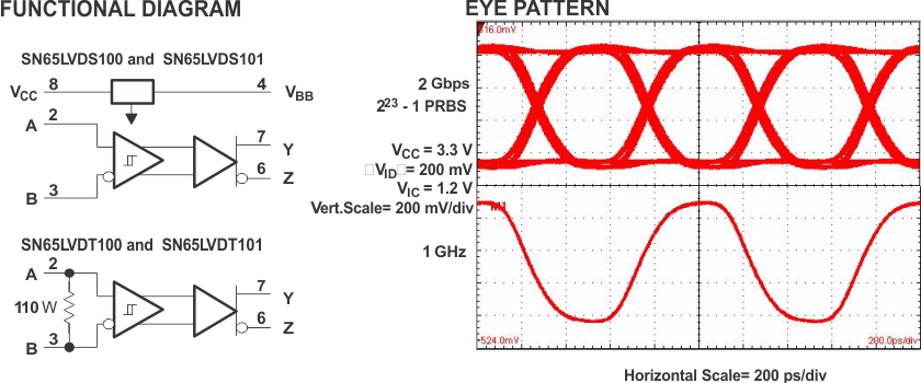
SN65LVDS100 SN65LVDT100 SN65LVDS101 SN65LVDT101 fbd_eye_lls516.gif