SLVAF04 October 2020 DRV8904-Q1 , DRV8906-Q1 , DRV8908-Q1 , DRV8910-Q1 , DRV8912-Q1
Application Brief
The DRV89XX-Q1 family of 4-, 6-, 8-, 10- and 12-channel motor drivers is designed to drive brushed motors, LEDs, and inductive loads. By utilizing SPI, each channel in the DRV89XX-Q1 family of devices can be independently configured to operate as a half-bridge, high-side switch, or low-side switch. Features such as the built-in PWM generator, enhanced open-load detection and both short to battery and ground protection makes this family of devices an attractive solution to drive many types of loads. This article examines how DRV89XX-Q1 devices can be used as a high-side or low-side switch to switch inductive loads such as relay coils or solenoids.
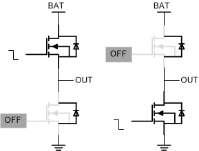
There is a difference in the circuit topology between the DRV89XX-Q1 as a high-side or low-side switch and a standard high-side or low-side switch. Figure 1 shows the DRV89XX-Q1 output MOSFETs. From this figure, it can be inferred that it is not possible to disconnect the body diode of the MOSFET that is not being used.
 Figure 1-1 DRV89xx-Q1 Output Circuit.
 Switching inductive loads
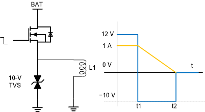
The switching of inductive loads deserves special attention because this operation may lead to high-voltage transients that can damage the switch. If a high-side switch is used to switch an inductor, a negative transient voltage is generated when the switch is turned off. Similarly, if the low side is used to power the inductor, then a positive transient voltage is generated. This is due to the stored magnetic energy in the inductor. To prevent damage when switching off the switch, the stored magnetic energy must be dissipated by clamping the voltage across the inductive load. Usually, a TVS diode or clamping circuit to clamp the voltage is used as Figure 2 shows.
 Figure 1-2 High-Side Switch Driving an Inductor.
 The choice of a suitable clamping voltage is
important – a higher clamping voltage will damage the driver circuit
and a lower clamping voltage will extend the current discharge time
of the inductor. Assuming that the inductor is ideal with inductance
L, clamping voltage is U; inductor current is I, and the duration it
takes for the inductor current to become zero after the switch is
turned off is T, the energy stored in the inductor at the instant
the switch is turned off is
WL = ½ × L
× I × I. The energy dissipated in the TVS diode is WTVS = ½ × U × I
× T. Equating these two expressions, ½ × U × I × T = ½ × L × I × I,
the time is given by the expression T = L × I / U. This formula
explains why high-side and low-side switches require higher clamping
voltage to reduce the current discharge time when driving inductive
loads.
Inductor current with smart high-side switches
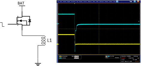
TI’s smart high-side switches, such as the TPS2HB16-Q1, are designed with clamping circuits that result in high clamping voltage. Note that this switch does not have a freewheeling diode. Figure 3 shows scope traces of the output voltage in cyan and inductor current in yellow after the switch is turned off. The load is a relay, with a coil current of 100 mA and the supply voltage to the high-side switch is 12 V. This figure shows that the time required for the inductor current to become zero is small. For more information, see How To Drive Resistive, Inductive, Capacitive, and Lighting Loads Application Report. The figure is an example when driving a relay using the TPS2HB16-Q1.
 Figure 1-3 Turning off Inductive Load With TPS2HB16-Q1.
 Inductor current with the DRV89xx-Q1
Because of the body diode in the MOSFET that is not being used, the DRV89XX-Q1 performs differently when switching off an inductive load. This is because the body diode acts as a freewheeling diode
Figure 4 shows scope traces of the output voltage in cyan and inductor current in yellow after the switch is turned off for the same relay.
 Figure 1-4 Turning off Inductive Load With DRV89xx-Q1.
 From Figure 4, it can be inferred that the freewheeling diode clamps the negative voltage of the inductor around -0.7 V, and the discharge of the inductor is about 3 ms.
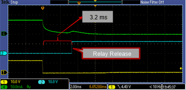
So what does this mean for the actual contact release? Figure 5 shows the scope trace of the relay coil current in green and the switch output voltage in cyan. The yellow trace in this figure is the switch output voltage.
 Figure 1-5 DRV8912-Q1 Driving a Relay Coil.
 From Figure 5, it can be inferred that the relay contacts are released 3 ms after the switch is turned off, which is less than the typical requirement of 10 ms for relay release in such applications.
Conclusions
DRV89xx-Q1 devices can be used as high-side or low-side switches to switch inductive loads in addition to being able to switch resistive loads and LEDs.