SLVS440C January 2003 – December 2014 TPS61045
PRODUCTION DATA.
- 1 Features
- 2 Applications
- 3 Description
- 4 Revision History
- 5 Pin Configuration and Functions
- 6 Specifications
- 7 Detailed Description
- 8 Application and Implementation
- 9 Power Supply Recommendations
- 10Layout
- 11Device and Documentation Support
- 12Mechanical, Packaging, and Orderable Information
1 Features
- Input Voltage Range from 1.8 to 6 V
- Output Voltage of up to 28 V Possible
- Up to 85% Efficiency
- Digitally Adjustable Output Voltage Control
- Disconnects Output From Input During Shutdown
- Switching Frequency up to 1 MHz
- No Load Quiescent Current 40 μA Typical
- Thermal Shutdown Mode
- Shutdown Current 0.1 μA Typical
- Available in Small 3-mm × 3-mm VSON Package
2 Applications
- LCD Bias Supply for Small to Medium LCD Displays
- OLED Display Power Supply
- PDA, Pocket PC, Smart Phones
- Handheld Devices
- Cellular Phones
3 Description
The TPS61045 device is a high-frequency boost converter with digitally-programmable output voltage and true shutdown. During shutdown, the output is disconnected from the input by opening the internal input switch. This allows a controlled power-up and power-down sequencing of the display. The output voltage can be increased or decreased in digital steps by applying a logic signal to the CTRL pin. The output voltage range, as well as the output voltage step size, can be programmed with the feedback divider network. With a high switching frequency of up to 1 MHz, the TPS61045 device allows the use of small external components, and together, with the small 8-pin VSON package, a minimum system solution size is achieved.
Device Information(1)
| PART NUMBER | PACKAGE | BODY SIZE (NOM) |
|---|---|---|
| TPS61045 | VSON (8) | 3.00 mm × 3.00 mm |
- For all available packages, see the orderable addendum at the end of the data sheet.
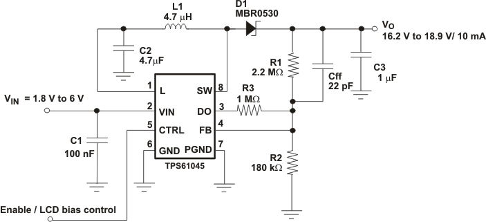
Simplified Schematic