SLVSFL2B May 2021 – December 2022 TPS7H4002-SP
PRODUCTION DATA
- 1 Features
- 2 Applications
- 3 Description
- 4 Revision History
- 5 Pin Configuration and Functions
- 6 Specifications
-
7 Detailed Description
- 7.1 Overview
- 7.2 Functional Block Diagram
- 7.3
Feature Description
- 7.3.1 VIN and Power VIN Pins (VIN and PVIN)
- 7.3.2 Voltage Reference
- 7.3.3 Adjusting the Output Voltage
- 7.3.4 Safe Start-Up Into Prebiased Outputs
- 7.3.5 Error Amplifier
- 7.3.6 Slope Compensation
- 7.3.7 Enable and Adjust UVLO
- 7.3.8 Adjustable Switching Frequency and Synchronization (SYNC)
- 7.3.9 Slow Start (SS/TR)
- 7.3.10 Power Good (PWRGD)
- 7.3.11 Sequencing (SS/TR)
- 7.3.12 Output Overvoltage Protection (OVP)
- 7.3.13 Overcurrent Protection
- 7.3.14 Thermal Shutdown
- 7.3.15 Turn-On Behavior
- 7.3.16 Small Signal Model for Frequency Compensation
- 7.4 Device Functional Modes
-
8 Application and Implementation
- 8.1 Application Information
- 8.2
Typical Application
- 8.2.1 Design Requirements
- 8.2.2
Detailed Design Procedure
- 8.2.2.1 Operating Frequency
- 8.2.2.2 Output Inductor Selection
- 8.2.2.3 Output Capacitor Selection
- 8.2.2.4 Output Schottky Diode
- 8.2.2.5 Slow Start Capacitor Selection
- 8.2.2.6 Undervoltage Lockout (UVLO) Set Point
- 8.2.2.7 Output Voltage Feedback Resistor Selection
- 8.2.2.8 Compensation Component Selection
- 8.2.3 Parallel Operation
- 8.2.4 Application Curve
- 9 Power Supply Recommendations
- 10Layout
- 11Device and Documentation Support
- 12Mechanical, Packaging, and Orderable Information
1 Features
- Radiation
performance:
- Radiation-hardness-assured up to
TID 100 krad(Si) - SEL, SEB, and SEGR immune
to
LET = 75 MeV-cm2/mg - SET and SEFI
characterized up to
LET = 75 MeV-cm2/mg
- Radiation-hardness-assured up to
- Peak efficiency: 96.9% (VO = 2.5 V)
- Integrated 50-mΩ and 35-mΩ MOSFETs
- Power rail: 3 to 5.5 V on VIN
- 3-A maximum output current
- Flexible switching frequency options:
- 100-kHz to 1-MHz adjustable internal oscillator
- External sync capability: 100 kHz to 1 MHz
- SYNC pin can be configured as a 500-kHz output for primary-secondary applications
- 0.807-V ±1.5% voltage reference over temperature, radiation, and line and load regulation
- Monotonic start-up into prebiased outputs
- Adjustable soft start through external capacitor
- Input enable and power-good output for power sequencing
- Power good output monitor for undervoltage and overvoltage
- Adjustable input undervoltage lockout (UVLO)
- 20-pin ultra-small, thermally-enhanced ceramic flatpack package (HKH) for space applications
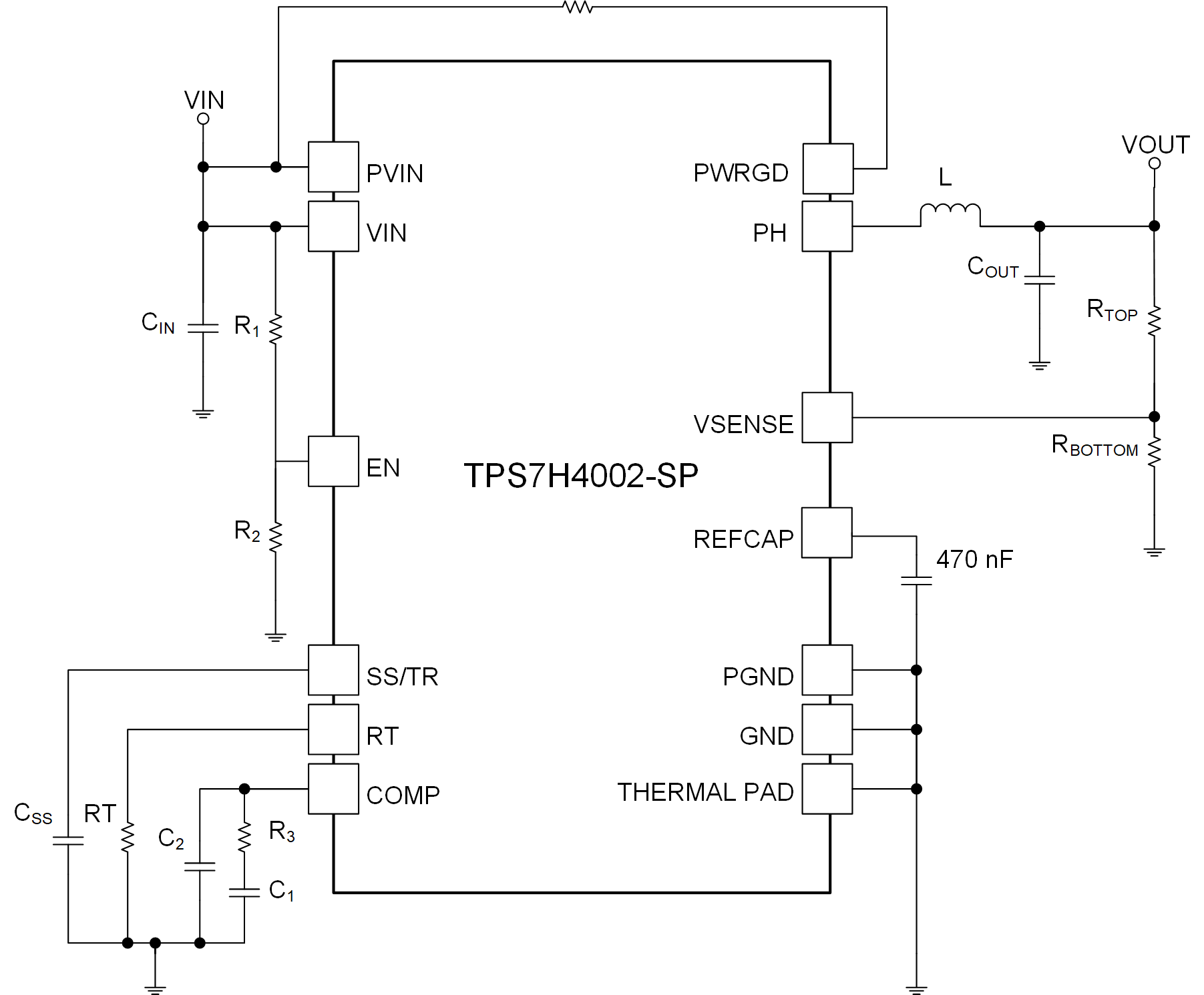
 Functional Diagram