SNAS348G May 2006 – April 2016 DAC124S085
PRODUCTION DATA.
- 1 Features
- 2 Applications
- 3 Description
- 4 Revision History
- 5 Description (continued)
- 6 Pin Configuration and Functions
- 7 Specifications
- 8 Detailed Description
- 9 Application and Implementation
- 10Power Supply Recommendations
- 11Layout
- 12Device and Documentation Support
- 13Mechanical, Packaging, and Orderable Information
1 Features
- Ensured Monotonicity
- Low Power Operation
- Rail-to-Rail Voltage Output
- Power-On Reset to 0 V
- Simultaneous Output Updating
- Wide Power Supply Range: 2.7 V to 5.5 V
- Industry's Smallest Package
- Power-Down Modes
- Resolution: 12 Bits
- INL: ±8 LSB (Maximum)
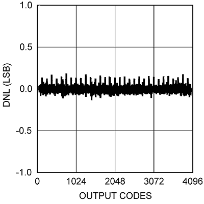
- DNL: 0.7 to −0.5 LSB (Maximum)
- Setting Time: 8.5 µs (Maximum)
- Zero Code Error: 15 mV (Maximum)
- Full-Scale Error: −0.75% FS (Maximum)
- Supply Power:
2 Applications
- Battery-Powered Instruments
- Digital Gain and Offset Adjustment
- Programmable Voltage and Current Sources
- Programmable Attenuators
3 Description
The DAC124S085 device is a full-featured, general-purpose, quad, 12-bit, voltage-output, digital-to-analog converter (DAC) that can operate from a single 2.7-V to 5.5-V supply and consumes 1.1 mW at 3 V and 2.4 mW at 5 V. The DAC124S085 is packaged in 10-pin WSON and VSSOP packages.
The 10-pin SON package makes the DAC124S085 the smallest quad DAC in its class. The on-chip output amplifier allows rail-to-rail output swing and the three-wire serial interface operates at clock rates up to 40 MHz over the entire supply voltage range. Competitive devices are limited to 25-MHz clock rates at supply voltages in the 2.7-V to 3.6-V range. The serial interface is compatible with standard SPI, QSPI, MICROWIRE, and DSP interfaces.
The reference for the DAC124S085 serves all four channels and can vary in voltage between 1 V and VA, providing the widest possible output dynamic range. The DAC124S085 has a 16-bit input shift register that controls the outputs to be updated, the mode of operation, the power-down condition, and the binary input data. All four outputs can be updated simultaneously or individually depending on the setting of the two mode of operation bits.
Device Information(1)
| PART NUMBER | PACKAGE | BODY SIZE (NOM) |
|---|---|---|
| DAC124S085 | VSSOP (10) | 3.00 mm × 3.00 mm |
| WSON (10) | 3.00 mm × 3.00 mm |
- For all available packages, see the orderable addendum at the end of the data sheet.
DNL at VA = 3 V
