SNVS970C March 2013 – October 2014 LM3279
PRODUCTION DATA.
- 1 Features
- 2 Applications
- 3 Description
- 4 Revision History
- 5 Pin Configuration and Functions
- 6 Specifications
- 7 Detailed Description
- 8 Application and Implementation
- 9 Power Supply Recommendations
- 10Layout
- 11Device and Documentation Support
- 12Mechanical, Packaging, and Orderable Information
Package Options
Mechanical Data (Package|Pins)
- YZR|16
Thermal pad, mechanical data (Package|Pins)
Orderable Information
1 Features
- MIPI® RFFE Digital Control Interface
- High-Efficiency PFM and PWM Modes with Internal Seamless Transition
- Operates from a Single Li-Ion Cell: 2.7 V to 5.5 V
- Adjustable Output Voltage:
- 1-A Maximum Load Capability for VBATT ≥ 3.2 V, VOUT = 3.6 V
- 2.4-MHz (typ.) Switching Frequency
- Seamless Buck-Boost Mode Transition
- Fast Output Voltage Transition: 0.8 V to 4 V in 20 µs
- High-Efficiency: 95% typ. at VBATT = 3.7 V,
VOUT = 3.3 V, at 300 mA - Input Overcurrent Limit
- Output Overvoltage Clamp
- Internal Compensation
2 Applications
- 3G/4G Smartphones
- RF PC Cards
- Tablets, eBooks Readers
- Battery-Powered RF Devices
3 Description
The LM3279 is a buck-boost DC/DC converter designed to generate output voltages above or below a given input voltage and is particularly suitable for Power Amplifiers operating from single-cell Li-Ion batteries in portable applications.
The LM3279 has four modes of operation: Pulse Width Modulation (PWM), Pulse Frequency Modulation (PFM), standby, and shutdown. During normal conditions, the LM3279 operates in full synchronous PWM mode at 2.4-MHz typical switching frequency, providing seamless transitions between buck and boost operating regimes. Energy-saving PFM mode increases efficiencies and current savings during low-power RF transmission modes. For high-transmit power, the device operates in PWM buck or boost mode, whereas the device can transition between PWM and PFM modes during low-power transmit. The LM3279 can be controlled either via an included MIPI RFFE Digital Control Interface or by using an analog control from an external MCU, offering design flexibility.
The power converter topology enables minimum total solution size by using one small footprint and case size inductor and two surface mount capacitors.
The LM3279 is internally compensated for buck and boost modes of operation thus providing an optimal transient response.
Device Information(1)
| PART NUMBER | PACKAGE | BODY SIZE (MAX) |
|---|---|---|
| LM3279 | DSBGA (16) | 2.529 mm x 2.146 mm |
- For all available packages, see the orderable addendum at the end of the datasheet.
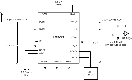
Simplified Schematic

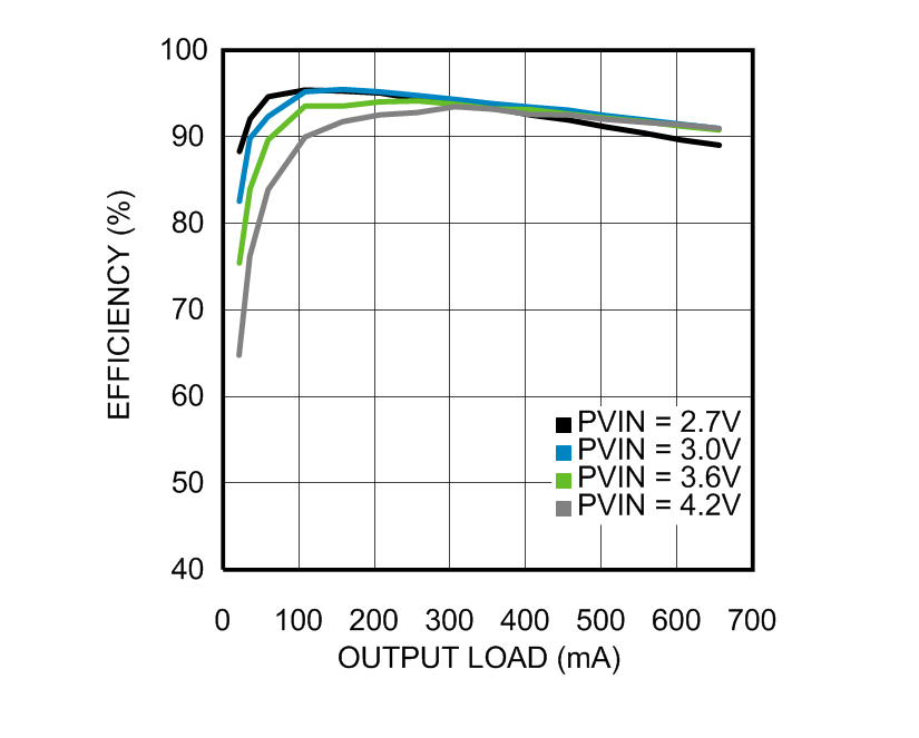
PWM Efficiency (VOUT = 2.4 V)
