SBAS758C January 2016 – September 2016 MUX508 , MUX509
PRODUCTION DATA.
- 1 Features
- 2 Applications
- 3 Description
- 4 Revision History
- 5 Device Comparison Table
- 6 Pin Configuration and Functions
- 7 Specifications
- 8 Parameter Measurement Information
- 9 Detailed Description
- 10Applications and Implementation
- 11Power-Supply Recommendations
- 12Layout
- 13Device and Documentation Support
- 14Mechanical, Packaging, and Orderable Information
Package Options
Mechanical Data (Package|Pins)
Thermal pad, mechanical data (Package|Pins)
Orderable Information
1 Features
- Low On-Capacitance
- Low Input Leakage: 10 pA
- Low Charge Injection: 0.3 pC
- Rail-to-Rail Operation
- Wide Supply Range: ±5 V to ±18 V, 10 V to 36 V
- Low On-Resistance: 125 Ω
- Transition Time: 92 ns
- Break-Before-Make Switching Action
- EN Pin Connectable to VDD
- Logic Levels: 2 V to VDD
- Low Supply Current: 45 µA
- ESD Protection HBM: 2000 V
- Industry-Standard TSSOP and SOIC Packages
2 Applications
- Factory Automation and Industrial Process Controls
- Programmable Logic Controllers (PLC)
- Analog Input Modules
- ATE Test Equipment
- Digital Multimeters
- Battery Monitoring Systems
3 Description
The MUX508 and MUX509 (MUX50x) are modern, complementary metal-oxide semiconductor (CMOS), analog multiplexers (muxes). The MUX508 offers 8:1 single-ended channels, whereas the MUX509 offers differential 4:1 or dual 4:1 single-ended channels. The MUX508 and MUX509 work equally well with either dual supplies (±5 V to ±18 V) or a single supply (10 V to 36 V). They also perform well with symmetric supplies (such as VDD = 12 V, VSS = –12 V), and unsymmetric supplies (such as VDD = 12 V, VSS = –5 V). All digital inputs have TTL-logic compatible thresholds, ensuring both TTL and CMOS logic compatibility when operating in the valid supply voltage range.
The MUX508 and MUX509 have very low on and off leakage currents, allowing these multiplexers to switch signals from high input impedance sources with minimal error. A low supply current of 45 µA allows for use in portable applications.
Device Information(1)
| PART NUMBER | PACKAGE | BODY SIZE (NOM) |
|---|---|---|
| MUX50x | TSSOP (16) | 5.00 mm × 4.40 mm |
| SOIC (16) | 9.90 mm × 3.91 mm |
- For all available packages, see the package option addendum at the end of the data sheet.
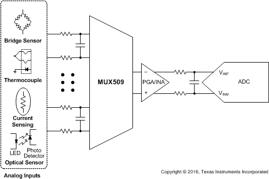
Simplified Schematic

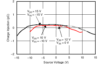
Charge Injection vs Source Voltage
