SBOS342C December 2008 – November 2015 OPA659
PRODUCTION DATA.
- 1 Features
- 2 Applications
- 3 Description
- 4 Revision History
- 5 Related Operational Amplifier Products
- 6 Pin Configuration and Functions
- 7 Specifications
- 8 Detailed Description
- 9 Application Information
- 10Power Supply Recommendations
- 11Layout
- 12Device and Documentation Support
- 13Mechanical, Packaging, and Orderable Information
Package Options
Mechanical Data (Package|Pins)
Thermal pad, mechanical data (Package|Pins)
- DRB|8
Orderable Information
1 Features
- High Bandwidth: 650 MHz (G = 1 V/V)
- High Slew Rate: 2550 V/μs (4-V Step)
- Excellent THD: –78 dBc at 10 MHz
- Low Input Voltage Noise: 8.9 nV/√Hz
- Fast Overdrive Recovery: 8 ns
- Fast Settling time (1% 4-V Step): 8 ns
- Low Input Offset Voltage: ±1 mV
- Low Input Bias Current: ±10 pA
- High Output Current: 70 mA
2 Applications
- High-Impedance Data Acquisition Input Amplifiers
- High-Impedance Oscilloscope Input Amplifiers
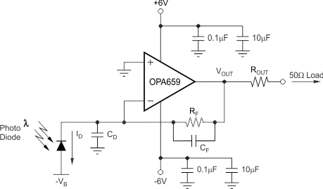
- Wideband Photodiode Transimpedance Amplifiers
- Wafer Scanning Equipment
- Optical Time-Domain Reflectometry (OTDR)
- High-Speed Time-of-Flight (TOF) Sensing
3 Description
The OPA659 combines a very wideband, unity-gain stable, voltage-feedback operational amplifier with a JFET-input stage to offer an ultra-high dynamic range amplifier for high impedance buffering in data acquisition applications such as oscilloscope front-end amplifiers and machine vision applications such as photodiode transimpedance amplifiers used in wafer inspection.
The wide 650-MHz unity-gain bandwidth is complemented by a very high 2550-V/μs slew rate.
The high input impedance and low bias current provided by the JFET input are supported by the low 8.9-nV/√Hz input voltage noise to achieve a very low integrated noise in wideband photodiode transimpedance applications.
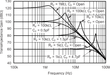
Broad transimpedance bandwidths are possible with the high 350-MHz gain bandwidth product of this device.
Where lower speed with lower quiescent current is required, consider the OPA656. Where unity-gain stability is not required, consider the OPA657.
Device Information(1)
| PART NUMBER | PACKAGE | BODY SIZE (NOM) |
|---|---|---|
| OPA659 | SOT-23 (5) | 2.90 mm × 1.60 mm |
| SON (8) | 3.00 mm × 3.00 mm |
- For all available packages, see the orderable addendum at the end of the data sheet.
Typical Application

Transimpedance Gain vs Frequency
