SLLSEH0F July 2013 – August 2014 SN65HVD01
PRODUCTION DATA.
- 1 Features
- 2 Applications
- 3 Description
- 4 Revision History
- 5 Pin Configuration and Functions
- 6 Specifications
- 7 Parameter Measurement Information
- 8 Detailed Description
- 9 Applications and Implementation
- 10Power Supply Recommendations
- 11Layout
- 12Device and Documentation Support
- 13Mechanical, Packaging, and Orderable Information
Package Options
Mechanical Data (Package|Pins)
- DRC|10
Thermal pad, mechanical data (Package|Pins)
- DRC|10
Orderable Information
1 Features
- Exceeds Requirements of TIA-485 Standard
- 1.65-V to 3.6-V Supply for Data and Enable Signals
- 3-V to 3.6-V Supply for Bus Signals
- SLR Pin Selectable Data Rates: 250 kbps or 20 Mbps
- 1/8th Unit Load to Support up to 256 Nodes on a Bus
- Small 3 mm x 3 mm SON Package
- Failsafe Receiver (Bus Open, Bus Shorted, Bus Idle)
- Operating Temperature Range: –40°C to 125°C
- Bus-Pin Protection More Than:
3 Description
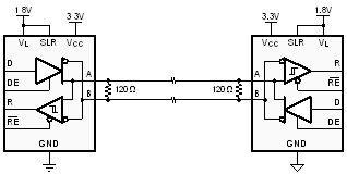
The SN65HVD01 is a low-power, 250 kbps or 20 Mbps data rate selectable RS-485 transceiver, utilizing a 1.65-V to 3.6-V supply for data and enable signals, and a 3.3 V ± 10% supply for bus signals. The device is designed for applications requiring synchronous (parallel transceiver) signal timing. On-chip transient suppression protects the device against destructive IEC 61000 ESD and EFT transients.
The device combines a differential driver and a differential receiver, connected internally to form a bus port suitable for half-duplex (two-wire bus) communication. The device features a wide common-mode voltage range making it suitable for multi-point applications over long cable runs. The SN65HVD01 is available in a tiny, 3 mm x 3 mm, SON package with operation characterized from -40°C to 125°C.