SCLS334J March 1996 – October 2014 SN74AHCT16244
PRODUCTION DATA.
- 1 Features
- 2 Applications
- 3 Description
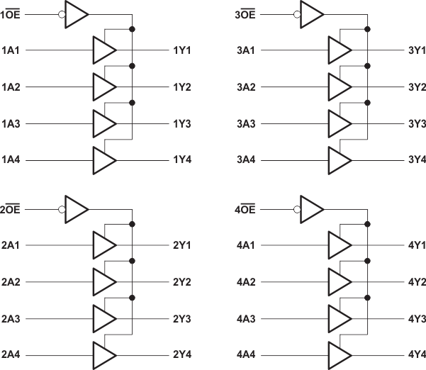
- 4 Simplified Schematic
- 5 Revision History
- 6 Pin Configuration and Functions
- 7 Specifications
- 8 Parameter Measurement Information
- 9 Detailed Description
- 10Application and Implementation
- 11Power Supply Recommendations
- 12Layout
- 13Device and Documentation Support
- 14Mechanical, Packaging, and Orderable Information
Package Options
Refer to the PDF data sheet for device specific package drawings
Mechanical Data (Package|Pins)
- DGG|48
- DL|48
- DGV|48
Thermal pad, mechanical data (Package|Pins)
Orderable Information
1 Features
- Members of the Texas Instruments Widebus™ Family
- EPIC™ (Enhanced-Performance Implanted CMOS) Process
- Inputs are TTL-Voltage Compatible
- Distributed VCC and GND Pins Minimize
High-Speed Switching Noise - Flow-Through Architecture Optimizes PCB Layout
- Latch-Up Performance Exceeds 250 mA
Per JESD 17 - ESD Protection Exceeds 2000 V Per
MIL-STD-883, Method 3015 - Package Options Include:
- Plastic Shrink Small Outline (DL) Package
- Thin Shrink Small Outline (DGG) Package
- Thin Very Small Outline (DGV) Package
- 380-mil Fine-Pitch Ceramic Flat (WD) Package Using 25-mil Center-to-Center Spacings
2 Applications
- Telecom Infrastructure
- Wireless Infrastructure
- Electronic Points of Sale
- Health and Fitness
- Printers and Other Peripherals
- Motor Drives
3 Description
The SN74AHCT16244 device is a 16-bit buffer and line driver specifically designed to improve the performance and density of 3-state memory address drivers, clock drivers, and bus-oriented receivers and transmitters.
Device Information(1)
| PART NUMBER | PACKAGE | BODY SIZE (NOM) |
|---|---|---|
| SN74AHCT16244 | TSSOP (48) | 12.50 mm x 6.10 mm |
| TVSOP (48) | 9.70 mm x 4.40 mm | |
| SSOP (48) | 15.80 mm x 7.50 mm |
- For all available packages, see the orderable addendum at the end of the data sheet.
4 Simplified Schematic