SLAS623A November 2008 – November 2016 TAS5342A
PRODUCTION DATA.
- 1 Features
- 2 Applications
- 3 Description
- 4 Revision History
- 5 Pin Configuration and Functions
- 6 Specifications
-
7 Detailed Description
- 7.1 Overview
- 7.2 Functional Block Diagram
- 7.3
Feature Description
- 7.3.1 Mid Z Sequence Compatibility
- 7.3.2 Device Protection System
- 7.3.3 Use Of TAS5342A In High-Modulation-Index Capable Systems
- 7.3.4 Overcurrent (OC) Protection With Current Limiting and Overload Detection
- 7.3.5 Pin-To-Pin Short Circuit Protection System (PPSC)
- 7.3.6 Overtemperature Protection
- 7.3.7 Undervoltage Protection (UVP) and Power-On Reset (POR)
- 7.3.8 Error Reporting
- 7.3.9 Device Reset
- 7.4 Device Functional Modes
- 8 Application and Implementation
- 9 Power Supply Recommendations
- 10Layout
- 11Device and Documentation Support
- 12Mechanical, Packaging, and Orderable Information
Package Options
Mechanical Data (Package|Pins)
- DDV|44
Thermal pad, mechanical data (Package|Pins)
- DDV|44
Orderable Information
1 Features
- Total Power Output (Bridge Tied Load)
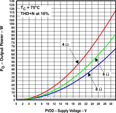
- 2 × 100 W at 10% THD+N Into 4 Ω
- 2 × 80 W at 10% THD+N Into 6 Ω
- 2 × 65 W at 10% THD+N Into 8 Ω
- Total Power Output (Single Ended)
- 4 × 40 W at 10% THD+N Into 3 Ω
- 4 × 30 W at 10% THD+N Into 4 Ω
- Total Power Output (Parallel Mode)
- 1 × 200 W at 10% THD+N Into 2 Ω
- 1 × 160 W at 10% THD+N Into 3 Ω
- >110 dB SNR (A-Weighted With TAS5518 Modulator)
- <0.1% THD+N (1 W, 1 kHz)
- Supports PWM Frame Rates of 192 kHz to
432 kHz - Resistor-Programmable Current Limit
- Integrated Self-Protection Circuitry, Including:
- Under Voltage Protection
- Overtemperature Warning and Error
- Overload Protection
- Short-Circuit Protection
- PWM Activity Detector
- Standalone Protection Recovery
- Power-On Reset (POR) to Eliminate System Power-Supply Sequencing
- High-Efficiency Power Stage (>90%) With 80-mΩ Output MOSFETs
- Thermally Enhanced Package 44-Pin HTSSOP (DDV)
- Error Reporting, 3.3-V and 5-V Compliant
- EMI Compliant When Used With Recommended System Design
2 Applications
- Mini/Micro Audio System
- DVD Receiver
- Home Theater
3 Description
The TAS5342A is a high-performance, integrated stereo digital amplifier power stage designed to drive a 4-Ω bridge-tied load (BTL) at up to 100 W per channel with low-harmonic distortion, low-integrated noise, and low-idle current.
The TAS5342A has a complete protection system integrated on-chip, safeguarding the device against a wide range of fault conditions that could damage the system. These protection features are short-circuit protection, over-current protection, under voltage protection, over temperature protection, and a loss of PWM signal (PWM activity detector).
A power-on-reset (POR) circuit is used to eliminate power-supply sequencing that is required for most power-stage designs.
Device Information(1)
| PART NUMBER | PACKAGE | BODY SIZE (NOM) |
|---|---|---|
| TAS5342A | HTSSOP (44) | 14.00 mm × 6.10 mm |
- For all available packages, see the orderable addendum at the end of the data sheet.
BTL Output Power vs Supply Voltage

4 Revision History
Changes from * Revision (November 2008) to A Revision
- Added Pin Configuration and Functions, Device Information table, ESD Ratings table, Feature Description section, Device Functional Modes, Application and Implementation section, Power Supply Recommendations section, Layout section, Device and Documentation Support section, and Mechanical, Packaging, and Orderable Information section Go
- Deleted the Ordering Information table; see the POA at the end of the datasheet. Go
- Added the Thermal Information tableGo