SLVS788D February 2009 – November 2016 TPS22951
PRODUCTION DATA.
- 1 Features
- 2 Applications
- 3 Description
- 4 Revision History
- 5 Pin Configurations and Functions
- 6 Specifications
- 7 Parameter Measurement Information
- 8 Detailed Description
- 9 Application and Implementation
- 10Power Supply Recommendations
- 11Layout
- 12Device and Documentation Support
- 13Mechanical, Packaging, and Orderable Information
Package Options
Mechanical Data (Package|Pins)
- YFP|6
Thermal pad, mechanical data (Package|Pins)
Orderable Information
1 Features
- 1-Ω P-Channel MOSFET
- 300-mA Continuous Source Current
- Thermal and Short-Circuit Protection
- 600-mA Current Limit
- Operating Range: VCC = 2.8 V to 5.3 V
- 41-μs Typical Rise Time
- 10-μA Maximum Standby Supply Current
- Ambient Temperature Range: –40°C to +85°C
- ESD Performance Tested Per JESD 22
- 4000-V Human-Body Model (HBM)
- 400-V Machine Model (MM)
- 1000-V Charged-Device Model (CDM)
2 Applications
- Smart Phones
- Notebooks
- Digital Cameras
- Peripheral Ports
3 Description
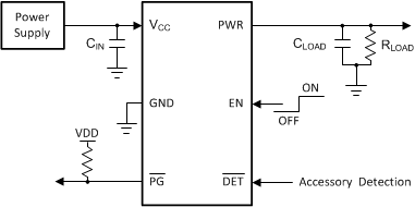
The TPS22951 smart-load switch is intended for applications where heavy capacitive loads and short circuits are likely to be encountered. This device incorporates a 1-Ω P-channel MOSFET power switch for power distribution. The switch is controlled by a logic enable (EN) input and an accessory detect (DET) pin. The switch is active when EN is high and DET is low. The switch is disabled if EN is low or DET is high. A low power state is achieved by driving EN low.
When the output load exceeds the current-limit threshold or a short is present, the device limits the output current to a safe level by increasing the on resistance of the power switch. When continuous heavy overloads and short circuits increase the power dissipation in the switch, causing the junction temperature to rise, a thermal-protection circuit shuts off the switch to prevent damage. The device recovers from a thermal shutdown once the device has cooled sufficiently, but the switch remains OFF until EN is toggled. This smart-load switch is designed to set current limit at 600 mA maximum.
Device Information(1)
| PART NUMBER | PACKAGE | BODY SIZE (NOM) |
|---|---|---|
| TPS22951 | DSBGA (6) | 1.20 mm x 0.80 mm |
- For all available packages, see the orderable addendum at the end of the data sheet.
Simplified Schematic
