SLUSBT2A January 2014 – August 2014 TPS51604-Q1
PRODUCTION DATA.
- 1 Features
- 2 Applications
- 3 Description
- 4 Revision History
- 5 Pin Configuration and Functions
- 6 Specifications
- 7 Detailed Description
- 8 Layout
- 9 Device and Documentation Support
- 10Mechanical, Packaging, and Orderable Information
Package Options
Mechanical Data (Package|Pins)
- DSG|8
Thermal pad, mechanical data (Package|Pins)
- DSG|8
Orderable Information
1 Features
- Qualified for Automotive Applications
- AEC-Q100 Qualified With the Following Results:
- Device Temperature Grade 1: –40°C to 125°C
- Device Human Body Model ESD Classification Level H2
- Device Charged Device Model ESD Classification Level C3B
- Reduced Dead-Time Drive Circuit for Optimized CCM
- Automatic Zero Crossing Detection for Optimized DCM Efficiency
- Multiple Low-Power Modes for Optimized Light-Load Efficiency
- Optimized Signal Path Delays for High-Frequency Operation
- Integrated BST Switch Drive Strength Optimized for Ultrabook FETs
- Optimized for 5-V FET Drive
- Conversion Input Voltage Range (VIN): 4.5 to 28 V
- 2-mm × 2-mm, 8-Pin, WSON Power-Pad Package
2 Applications
- Automotive Rear Seat Entertainment (RSE) Tablets Using High-Frequency CPUs With the Following Power Input:
- Adapter
- Battery
- NVDC
- 5-V or 12-V Rails
3 Description
The TPS51604-Q1 drivers are optimized for high-frequency CPU VCORE applications. Advanced features such as reduced dead-time drive and auto zero crossing are used to optimize efficiency over the entire load range.
The SKIP pin provides immediate CCM operation to support controlled management of the output voltage. In addition, the TPS51604-Q1 supports two low-power modes. With the PWM input in 3-state, quiescent current is reduced to 130 µA, with immediate response. When SKIP is held at 3-state, the current is reduced to 8 µA (typically 20 µs is required to resume switching). Paired with the appropriate TI controller, the drivers deliver an exceptionally high performance power supply system.
The TPS51604-Q1 device is packaged in a space saving, thermally-enhanced 8-pin, 2-mm x 2-mm WSON package and operates from –40°C to 125°C.
Device Information(1)
| PART NUMBER | PACKAGE | BODY SIZE (NOM) |
|---|---|---|
| TPS51604-Q1 | WSON (8) | 2.00 mm × 2.00 mm |
- For all available packages, see the orderable addendum at the end of the data sheet.
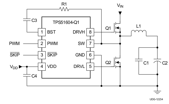
Simplified Schematic