SLVSB01D October 2011 – August 2016 TPS54295
PRODUCTION DATA.
- 1 Features
- 2 Applications
- 3 Description
- 4 Revision History
- 5 Pin Configuration and Functions
- 6 Specifications
- 7 Detailed Description
- 8 Application and Implementation
- 9 Power Supply Recommendations
- 10Layout
- 11Device and Documentation Support
- 12Mechanical, Packaging, and Orderable Information
Package Options
Mechanical Data (Package|Pins)
Thermal pad, mechanical data (Package|Pins)
Orderable Information
1 Features
- D-CAP2™ Control Mode
- Fast Transient Response
- No External Parts Required For Loop Compensation
- Compatible With Ceramic Output Capacitors
- Wide Input Voltage Range : 4.5 V to 18 V
- Output Voltage Range : 0.76 V to 7 V
- Highly Efficient Integrated FETs Optimized for Low Duty Cycle Applications
- 150 mΩ (High-Side) and 100 mΩ (Low-Side)
- High Initial Reference Accuracy
- Low-Side rDS(ON) Lossless Current Sensing
- Adjustable Soft Start
- Non-Sinking Prebiased Soft Start
- 700-kHz Switching Frequency
- Cycle-by-Cycle Overcurrent Limit Control
- OCL, OVP, UVP, UVLO, and TSD Protections
- Adaptive Gate Drivers With Integrated Boost PMOS Switch
- OCP Constant Due to Thermally Compensated rDS(ON) With 4000 ppm/℃
- 16-Pin HTSSOP, 16-pin VQFN
- Auto-Skip Eco-mode™ for High Efficiency at Light Load
2 Applications
- Point-of-Load Regulation in Low Power Systems for Wide Range of Applications
- Digital TV Power Supplies
- Networking Home Terminals
- Digital Set Top Boxes (STB)
- DVD Players and Recorders
- Gaming Consoles and Other
3 Description
The TPS54295 is a dual, adaptive on-time D-CAP2 mode synchronous buck converter. The TPS54295 enables system designers to complete the suite of various end-equipment power bus regulators with a cost effective, low component count, and low standby current solution. The main control loops of the TPS54295 use the D-CAP2 mode control which provides a very fast transient response with no external compensation components. The adaptive on-time control supports seamless transition between PWM mode at higher load conditions and Eco-mode operation at light loads. Eco-mode allows the TPS54295 to maintain high efficiency during lighter load conditions. The TPS54295 is able to adapt to both low equivalent series resistance (ESR) output capacitors such as POSCAP or SP-CAP, and ultra-low ESR ceramic capacitors. The device provides convenient and efficient operation with input voltages from 4.5 V to 18 V.
The TPS54295 is available in a 4.4 mm × 5 mm 16-pin HTSSOP (PWP) package and 4 mm x 4 mm 16-pin VQFN (RSA) package, designed to operate at an ambient temperature range from –40°C to 85°C.
Device Information(1)
| PART NUMBER | PACKAGE | BODY SIZE (NOM) |
|---|---|---|
| TPS54295 | HTSSOP (16) | 5.00 mm × 4.40 mm |
| VQFN (16) | 4.00 mm × 4.00 mm |
- For all available packages, see the orderable addendum at the end of the data sheet.
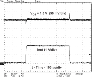
Load Transient Response
