SLVS400D August 2001 – January 2015 TPS54611 , TPS54612 , TPS54613 , TPS54614 , TPS54615 , TPS54616
PRODUCTION DATA.
- 1 Features
- 2 Applications
- 3 Description
- 4 Revision History
- 5 Pin Configuration and Functions
- 6 Specifications
-
7 Detailed Description
- 7.1 Overview
- 7.2 Functional Block Diagram
- 7.3
Feature Description
- 7.3.1 Undervoltage Lock Out (UVLO)
- 7.3.2 Slow-Start and Enable (SS/ENA)
- 7.3.3 VBIAS Regulator
- 7.3.4 Voltage Reference
- 7.3.5 Oscillator and PWM Ramp
- 7.3.6 Error Amplifier
- 7.3.7 PWM Control
- 7.3.8 Dead-Time Control and MOSFET Drivers
- 7.3.9 Overcurrent Protection
- 7.3.10 Thermal Shutdown
- 7.3.11 Powergood (PWRGD)
- 7.4 Device Functional Modes
- 8 Application and Implementation
- 9 Power Supply Recommendations
- 10Layout
- 11Device and Documentation Support
- 12Mechanical, Packaging, and Orderable Information
Package Options
Mechanical Data (Package|Pins)
- PWP|28
Thermal pad, mechanical data (Package|Pins)
- PWP|28
Orderable Information
1 Features
- 30-mΩ, 12-A Peak MOSFET Switches for High Efficiency at 6-A Continuous Output Source and Sink
- 0.9-V, 1.2-V, 1.5-V, 1.8-V, 2.5-V, and 3.3-V Fixed Output Voltage Devices With 1.0% Initial Accuracy
- Internally Compensated for Easy Use and Minimal Component Count
- Fast Transient Response
- Wide PWM Frequency − Fixed 350 kHz, 550 kHz or Adjustable 280 kHz to 700 kHz
- Load Protected by Peak Current Limit and Thermal Shutdown
- Integrated Solution Reduces Board Area and Total Cost
2 Applications
- Low-Voltage, High-Density Systems With Power Distributed at 5 V or 3.3 V
- Point of Load Regulation for High Performance DSPs, FPGAs, ASICs and Microprocessors
- Broadband, Networking and Optical Communications Infrastructure
- Portable Computing/Notebook PCs
3 Description
The SWIFT™ family of dc/dc regulators, the TPS54611, TPS54612, TPS54613, TPS54614, TPS54615 and TPS54616 low-input voltage high-output current synchronous-buck PWM converters integrate all required active components. Included on the substrate are true, high-performance, voltage error amplifiers that provide high performance under transient conditions; an under-voltage-lockout circuit to prevent start-up until the input voltage reaches 3 V; an internally and externally set slow-start circuit to limit in-rush currents; and a powergood output useful for processor/logic reset, fault signaling, and supply sequencing.
The TPS5461x devices are available in a thermally enhanced 28-pin TSSOP (PWP) PowerPAD™ package, which eliminates bulky heatsinks. TI provides evaluation modules and the SWIFT™ designer software tool to aid in quickly achieving high-performance power supply designs to meet aggressive equipment development cycles.
Device Information(1)
| PART NUMBER | PACKAGE | OUTPUT VOLTAGE |
|---|---|---|
| TPS54611 | HTSSOP (28) | 0.9 V |
| TPS54612 | 1.2 V | |
| TPS54613 | 1.5 V | |
| TPS54614 | 1.8 V | |
| TPS54615 | 2.5 V | |
| TPS54616 | 3.3 V |
- For all available packages, see the orderable addendum at the end of the datasheet.
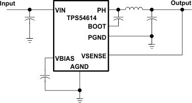
Simplified Schematic
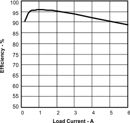
Efficiency at 350 kHz