SLVS314F SEPTEMBER 2000 – August 2015 TPS61010 , TPS61012 , TPS61013 , TPS61014 , TPS61015 , TPS61016
PRODUCTION DATA.
- 1 Features
- 2 Applications
- 3 Description
- 4 Revision History
- 5 Device Comparison Table
- 6 Pin Configuration and Functions
- 7 Specifications
- 8 Parameter Measurement Information
- 9 Detailed Description
-
10Application and Implementation
- 10.1 Application Information
- 10.2
Typical Applications
- 10.2.1 1.8-mm Maximum Height Power Supply With Single Battery Cell Input Using Low Profile Components
- 10.2.2 250-mA Power Supply With Two Battery Cell Input
- 10.2.3 Dual Output Voltage Power Supply for DSPs
- 10.2.4 Power Supply With Auxiliary Positive Output Voltage
- 10.2.5 Power Supply With Auxiliary Negative Output Voltage
- 10.2.6 TPS6101x EVM Circuit Diagram
- 11Power Supply Recommendations
- 12Layout
- 13Device and Documentation Support
- 14Mechanical, Packaging, and Orderable Information
Package Options
Refer to the PDF data sheet for device specific package drawings
Mechanical Data (Package|Pins)
- DGS|10
Thermal pad, mechanical data (Package|Pins)
Orderable Information
1 Features
- Integrated Synchronous Rectifier for Highest Power Conversion Efficiency (> 95%)
- Start-Up Into Full Load With Supply Voltages as Low as 0.9 V, Operating Down to 0.8 V
- 200-mA Output Current From 0.9-V Supply
- Powersave-Mode for Improved Efficiency at Low Output Currents
- Autodischarge Allows to Discharge Output Capacitor During Shutdown
- Device Quiescent Current Less Than 50 μA
- Ease-of-Use Through Isolation of Load From Battery During Shutdown of Converter
- Integrated Antiringing Switch Across Inductor
- Integrated Low Battery Comparator
- Micro-Small 10-Pin MSOP or 3 mm x 3 mm QFN Package
- EVM Available (TPS6101xEVM-157)
2 Applications
- All Single- or Dual-Cell Battery Operated Products
- Internet Audio Players
- Pager
- Portable Medical Diagnostic Equipment
- Remote Control
- Wireless Headsets
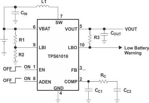
Simplified Application Circuit

3 Description
The TPS6101x devices are boost converters intended for systems that are typically operated from a single- or dual-cell nickel-cadmium (NiCd), nickel-metal hydride (NiMH), or alkaline battery.
The converter output voltage can be adjusted from 1.5 V to a maximum of 3.3 V, by an external resistor divider or, is fixed internally on the chip. The devices provide an output current of 200 mA with a supply voltage of only 0.9 V. The converter starts up into a full load with a supply voltage of only 0.9 V and stays in operation with supply voltages down to 0.8 V.
The converter is based on a fixed frequency, current mode, pulse-width-modulation (PWM) controller that goes automatically into power save mode at light load. It uses a built-in synchronous rectifier, so, no external Schottky diode is required and the system efficiency is improved. The current through the switch is limited to a maximum value of 1300 mA. The converter can be disabled to minimize battery drain. During shutdown, the load is completely isolated from the battery.
An autodischarge function allows discharging the output capacitor during shutdown mode. This is especially useful when a microcontroller or memory is supplied, where residual voltage across the output capacitor can cause malfunction of the applications. When programming the ADEN-pin, the autodischarge function can be disabled. A low-EMI mode is implemented to reduce interference and radiated electromagnetic energy when the converter enters the discontinuous conduction mode. The device is packaged in the micro-small space saving 10-pin MSOP package. The TPS61010 is also available in a 3 mm x 3 mm 10-pin QFN package.
Device Information(1)
| PART NUMBER | PACKAGE | BODY SIZE (NOM) |
|---|---|---|
| TPS61010 | VSSOP (10) | 3.00 mm x 3.00 mm |
| VSON (10) | ||
| TPS61011 | VSSOP (10) | 3.00 mm x 3.00 mm |
| TPS61012 | ||
| TPS61013 | ||
| TPS61014 | ||
| TPS61015 | ||
| TPS61016 |
- For all available packages, see the orderable addendum at the end of the datasheet.