SLVSAT8E November 2011 – May 2017 TPS62170 , TPS62171 , TPS62172 , TPS62173
PRODUCTION DATA.
- 1 Features
- 2 Applications
- 3 Description
- 4 Revision History
- 5 Device Voltage Options
- 6 Pin Configuration and Functions
- 7 Specifications
- 8 Detailed Description
-
9 Application and Implementation
- 9.1 Application Information
- 9.2
Typical Application
- 9.2.1 Design Requirements
- 9.2.2 Detailed Design Procedure
- 9.2.3 Application Curves
- 9.3 System Examples
- 10Power Supply Recommendations
- 11Layout
- 12Device and Documentation Support
- 13Mechanical, Packaging, and Orderable Information
Package Options
Mechanical Data (Package|Pins)
- DSG|8
Thermal pad, mechanical data (Package|Pins)
- DSG|8
Orderable Information
1 Features
- DCS-Control™ Topology
- Input Voltage Range from 3 V to 17 V
- Up to 500-mA Output Current
- Adjustable Output Voltage from 0.9 V to 6 V
- Fixed Output Voltage Versions
- Seamless Power Save Mode Transition
- Typically 17-µA Quiescent Current
- Power Good Output
- 100% Duty Cycle Mode
- Short Circuit Protection
- Over Temperature Protection
- Pin to Pin Compatible with TPS62160 and TPS62125
- Available in a 2-mm × 2-mm 8-Pin WSON Package
- Create a Custom Design using the TPS62170 with the WEBENCH® Power Designer
2 Applications
- Standard 12-V Rail Supplies
- POL Supply from Single or Multiple Li-Ion Battery
- LDO Replacement
- Embedded Systems
- Digital Still Camera, Video
- Mobile PCs, Tablet-PCs, Modems
3 Description
The TPS6217x device family are easy to use synchronous step-down DC-DC converters optimized for applications with high power density. A high switching frequency of typically 2.25 MHz allows the use of small inductors and provides fast transient response as well as high output voltage accuracy by utilization of the DCS-Control™ topology.
With its wide operating input voltage range of 3 V to 17 V, the devices are ideally suited for systems powered from either a Li-Ion or other battery as well as from 12-V intermediate power rails. It supports up to 0.5-A continuous output current at output voltages between 0.9 V and 6 V (with 100% duty cycle mode).
Power sequencing is also possible by configuring the enable and open-drain power good pins.
In power save mode, the devices show quiescent current of about 17 μA from VIN. Power save mode, entered automatically and seamlessly if the load is small, maintains high efficiency over the entire load range. In shutdown mode, the device is turned off and shutdown current consumption is less than 2 μA.
The device, available in adjustable and fixed output voltage versions, is packaged in a 2-mm × 2-mm 8-pin WSON package (DSG).
Device Information(1)
| PART NUMBER | PACKAGE | BODY SIZE (NOM) |
|---|---|---|
| TPS6217x | WSON (8) | 2.00 mm x 2.00 mm |
- For all available packages, see the orderable addendum at the end of the datasheet.
Typical Application Schematic

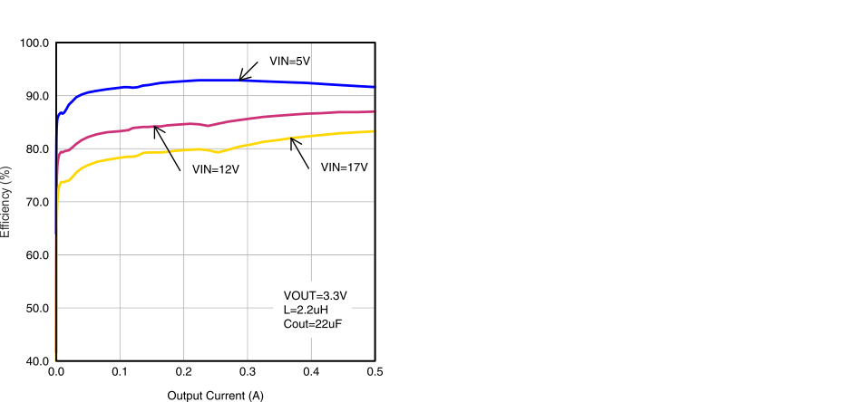
Efficiency vs Output Current
